EasyManua.ls Logo

Sharp CE-150 - Page 312

Sharp CE-150
412 pages
Print Icon
To Next Page IconTo Next Page
To Previous Page IconTo Previous Page
Loading...
72
A
ll
and more about Sharp PC-1500
at
http://
www
.PC-1500.info
CD
DOB r
eg
ist
er
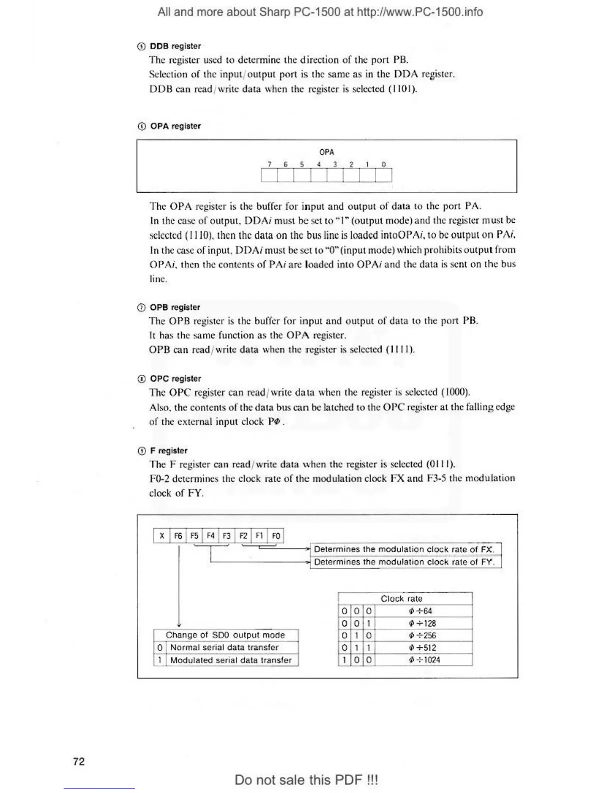
The
register used
IO
determine
the
direction
of
the port PB.
Selection
of
the
inpm
/outplll
port
is the
sa
me as in the
DDA
resister.
DDB
can
r
ead
/ write
data
when the register is selected ( I
10
1).
© OPA r
eg
ister
OPA
7 6 5 • 3
~
0
,_,__LI_! I I
The
OPA
register
is
the buffer for input
and
outpu
t
of
di
1rn
to the port
PA
.
Jn
the case
of
output.
DD
Ai
mu
st
be
set to
..
I"
(o
ut
put
mode)
and
the regist
er
must be
sele
cted
(
111
0)
,
then
th
e
data
on
th
e
bus
line is lo
aded
intoOPr'\i,
Hl
be
output
on
P/1i.
Jn
t
he
case
of
input.
DD
Ai must be set
to
"O"(input mode) which prohibits
outpu
t from
OPAi.
then the contents of
PAi
arc
loaded into
OPA
i
and
the
data
is sent
on
th
e bus
line.
<D
OPB register
Th
e
OPB
register is the buffer
fo
r input
and
o utput
of
da
ta
to the port PB.
It has the
same
fu
nction
as
the O
PA
1·egister.
OPB
can
re
ad
/ write
data
when
the
regist
er
is selected (I I I I).
© OPC register
Th
e
OP
C register
can
read/write
data
when the regis
ter
is
selected (
IOOO).
Al
so
.
the
contents
of
the
data
bus
can
be latched
to
the
OPC
regi~tcr
at
the falli
ng
edge
of
the external input clock
P4>.
@ F
reg
ister
Th
e F register
can
read/ write
data
when the regi
st
er
is selected
(OJ
I I).
F0
-2
de
t
erm
i
ne
s the clock rate
of
the
modulation clock FX
and
F3-5 the
modulation
clock
of
FY
.
x
_L
F6J
ro
J
F4
_1
F3J
F2
J n J
Fo
_I
I
Determines the modula
ti
on clock tate
of
FX,
Determines the
modu
lation cl
ock
rate
of
FY.
I
Clock ra
te
0 0 0
1'
+64
0 0
1
4>+
128
Change of
SOO
outpu
t moae
~
'
t
0
,p
+256
0
Notma
l serial data transfer
0 1 1
,p
+5
12
I
f\
1odul
ate
d serial
data
transfer
1 0 0
ol
+ 1
024
Do
not sale this
PDF!!!