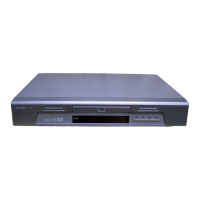
DV-600S
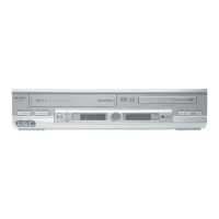
DV-600H
11-17
35 CLK System Clock Active on the positive going edge to sample all inputs.
18 CS Chip Select Disables or enables device operation by masking or enabling all inputs
except CLK. CKE and L(U)DQM
34 CKE Clock Enable Masks system clock to freeze operation from the next clock cycle.
CKE should be enabled at least one cycle prior to new command.
Disable input buffers for power down in stanby.
21~24 A0~A10/AP Address Row/column address are multiplexed on the same pins.
27~32 Row address: RA0~RA10, column address: CA0~CA7
20
19 BA Bank Select Address Selects bank to be activated during row address latch time.
Selects bank for read/write during clumn address latch time.
17 RAS Row Address Strobe Latches row address on the positive going edge of the CLK with RAS low.
Enables row access & precharge.
16 CAS Column Address Strobe Latches addresses on the positive going edge of the CLK with CAS low.
Enables row access.
15 WE Write Enable Enable write operation and row precharge.
Latches data in starting from CAS, WE active.
14, 36 L(U)DOM Data Input/Output Mask Makes data output Hi-Z, tsHZ after the clock and masks the output.
Blocks data input when L(U)DQM active.
2, 3, 5, DQ0~15 Data Input/Output Data inputs/outputs are multiplexed on the same pins.
6, 8, 9, 11, 12, 39, 40,
42, 43, 45, 46, 48, 49
Vcc/Vss Power Supply/Ground Power and ground for the input buffers and the core logic.
25, 1/26, 50
Vcc/VssO
Data Output Power/Ground
Isolated power supply and ground for the output buffers to provide
44, 38, 13, 7/4, 10, 41, 47 improved noise immunity.
37 NC/RFU No Connection/ This pin is recommanded to be left No Connection on the device
Reserved for Future Use
11-13. IC602 IX1537GE 16M SDARM
Terminal
Terminal Name Name Input Function
CLK
CLK
CKE
CS RAS CAS
WE
ADD
LCKE
Address Register
Bank Select
Row Buffer
Refrsh Counter
Rown Decorder
Col. Buffer
LRAS
LRAS
LCBR
LCBR
LWE
LCAS
L(U)DCM
Timing Register
LWCBR
LDQM
Programming Resiter
Latency & Burst Length
Column Decoder
Data Input Register
512K x 16
512K x 16
Sense AMP
I/O Control
Output Buffer
LWE
LDQM
DQi
• Samsung Electronics reserves the right to
change products or specification without
• Block Diagram