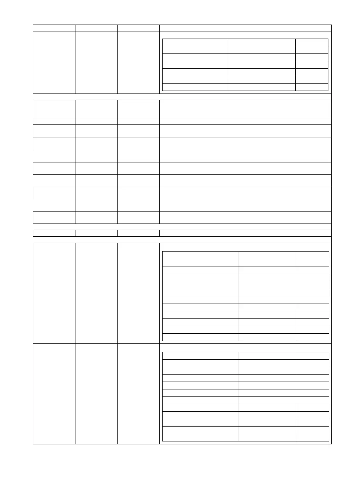
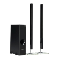
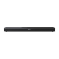
HT-DV40H
8 – 24
UA0_TX/GPIO 206 Input/Output UART #0 data transmit or GPIO
V_COMP 207 A
Compensation pin. A 0.1pF ceramic capacitor must be used to bypass this pin to
VSSA.
The lead length must be kept as short as possible to avoid noise.
V_BIAS 208
V_FSADJ 209 A
Full-Scale adjustment control pin. The full-scale current of D/A converters can be
adjusted by connecting a resistor (R
SET
) between this pin and ground.
V_REFOUT 210 A
Voltage reference output. It generates typical 1.2V voltage reference and may be
used to drive V_REFIN pin directly.
V_DAC[0] 211 A
Video DAC output #0. This is a high-impedance current source output. These
outputs can drive a 37.5Ω load directly.
V_DAC[1] 214 A
Video DAC output #1. This is a high-impedance current source output. These
outputs can drive a 37.5Ω load directly.
V_DAC[2] (or NC) 215 A
Video DAC output #2. This is a high-impedance current source output. These
outputs can drive a 37.5Ω load directly. NC for SPHE8281A-256.
V_DAC[3] (or NC) 218 A
Video DAC output #3. This is a high-impedance current source output. These
outputs can drive a 37.5Ω load directly. NC for SPHE8281A-256.
V_DAC[4] 219 A
Video DAC output #4. This is a high-impedance current source output. These
outputs can drive a 37.5Ω load directly.
V_DAC[5] 221 A
Video DAC output #5. This is a high-impedance current source output. These
outputs can drive a 37.5Ω load directly.
NC 223 - No connection
R_A20/GPIO 225 Input/Output
ROM / SRAM / flash address bus bit [20], or GPIO[92]
R_A21/GPIO 226 Input/Output
ROM / SRAM / flash address bus bit [21], or GPIO[93]
Symbol Pin # Input/Output Description
Priority selection Function Dir
gpio_first[3][13] = 1 GPIO[61] Input/Output
sft_cfg2[3:2] = 1 UA0_TXD (default) Input
sft_cfg3[13:12] = 1 TV_VSYNC Input/Output
sft_cfg14[10:8] = 3'b011 TV_VDSYNC_SRGB Output
sft_cfg4[15:13] = 3'b011 TV_VSYNC_PC Output
(other) GPIO[61] Input/Output
Priority selection Function Dir
gpio_first[5][12] = 1
GPIO[92]
Input/Output
PINMUX_control[0][1] = 1
ROM_ADDR[20] (default)
Output
{sft_cfg20[0],sft_cfg7[5:4]} = 3'b010
656_DATA[7]
Output
{sft_cfg20[1],sft_cfg19[5:4]} = 3'b010
HD_DATA[7]
Output
{sft_cfg20[2],sft_cfg14[7:6]} = 3'b010
SRGB_DATA[7]
Output
sft_cfg11[5:3] = 3'b110
TS_GNT_B
Input/Output
sft_cfg0[13:12] = 3
TV_LCD_B[0]
Output
sfg_cfg16[15:12] = 4'b0010
FM_GPIOB[14]
Input/Output
sfg_cfg16[15:12] = 4'b0110
FM_GPIOB[12]
Input/Output
sfg_cfg18[3:0] = 4'b1000
FM_GPIOB[34]
Input/Output
(other)
GPIO[92]
Input/Output
Priority selection Function Dir
gpio_first[5][13] = 1
GPIO[93]
Input/Output
PINMUX_control[0][2] = 1
ROM_ADDR[21] (default)
Input/Output
{sft_cfg20[0],sft_cfg7[5:4]} = 3'b010
656_DATA[6]
Output
{sft_cfg20[1],sft_cfg19[5:4]} = 3'b010
HD_DATA[6]
Output
{sft_cfg20[2],sft_cfg14[7:6]} = 3'b010
SRGB_DATA[6]
Output
sft_cfg11[5:3] = 3'b110
TS_FRAME_B
Input/Output
sft_cfg0[13:12] = 3
TV_LCD_B[1]
Output
sfg_cfg16[11:8] = 4'b0110
FM_GPIOB[11]
Input/Output
sfg_cfg16[15:12] = 4'b0010
FM_GPIOB[15]
Input/Output
sfg_cfg18[3:0] = 4'b1000
FM_GPIOB[33]
Input/Output
(other)
GPIO[93]
Input/Output