47
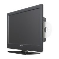
LC-22DV510
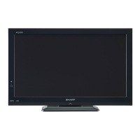
LC-24DV510
12. DDR2 SDRAM 8M × 4 BANKS × 16 BIT (W9751G6JB) (U154, U155)
12.1. General Description
The W9751G6JB is a 512M bits DDR2 SDRAM, organized as 8,388,608 words × 4 banks × 16 bits. This device
achieves high speed transfer rates up to 1066Mb/sec/pin (DDR2-1066) for general applications.
W9751G6JB is sorted into the following speed grades: -18, -25 and -3. The -18 is compliant to the DDR2-
1066/CL7 specification. The -25 is compliant to the DDR2-800 (5-5-5) or DDR2-800 (6-6-6) specification.
The -3 is compliant to the DDR2-667 (5-5-5) specification. All of the control and address inputs are
synchronized with a pair of externally supplied differential clocks. Inputs are latched at the cross point of
differential clocks (CLK rising and CLK falling). All I/Os are synchronized with a single ended DQS or
differential DQS- DQS pair in a source synchronous fashion.
12.2. Features
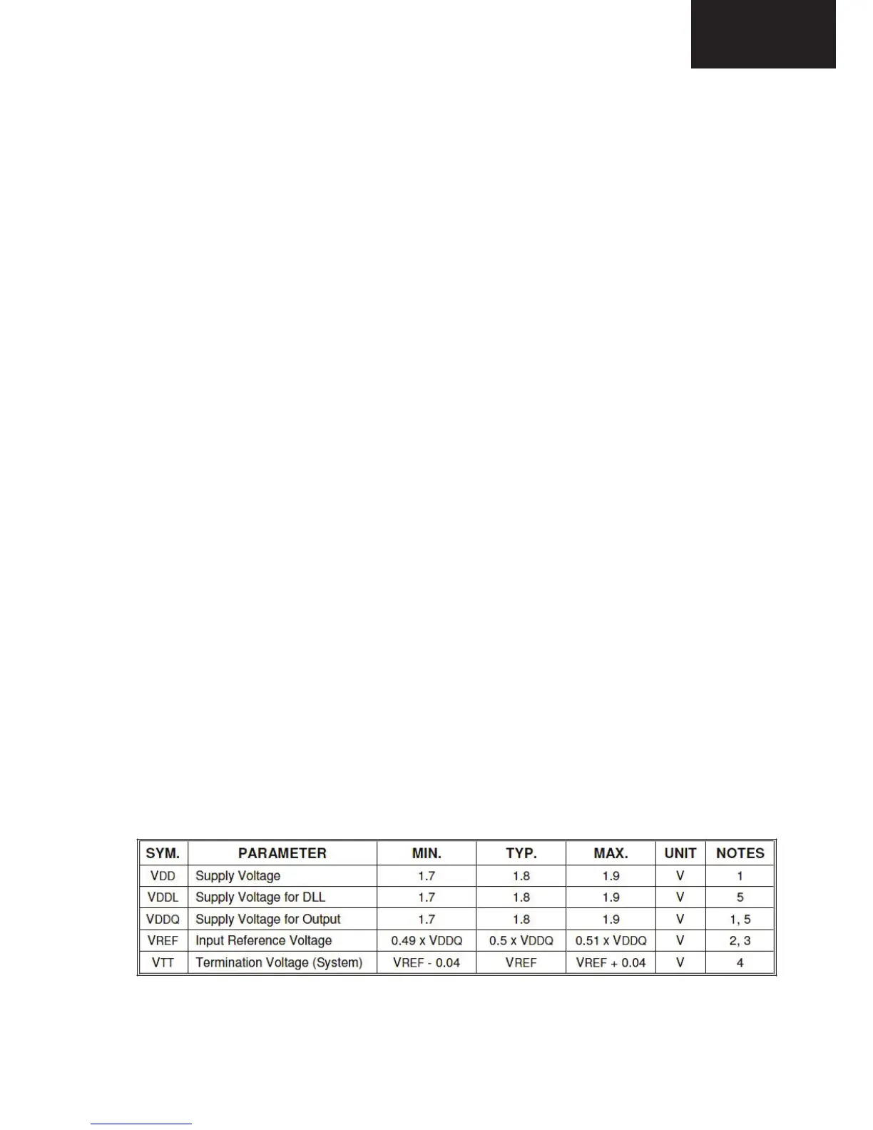
Power Supply: VDD, VDDQ = 1.8 V± 0.1 V
Double Data Rate architecture: two data transfers per clock cycle
CAS Latency: 3, 4, 5, 6 and 7
Burst Length: 4 and 8
Bi-directional, differential data strobes are transmitted / received with data
Edge-aligned with Read data and center-aligned with Write data
DLL aligns DQ and DQS transitions with clock
Differential clock inputs (CLK and CLK )
Data masks (DM) for write data
Commands entered on each positive CLK edge, data and data mask are referenced to both
edges of DQS
Posted CAS programmable additive latency supported to make command and data bus
efficiency
Read Latency = Additive Latency plus CAS Latency (RL = AL + CL)
Off-Chip-Driver impedance adjustment (OCD) and On-Die-Termination (ODT) for better
signal quality
Auto-precharge operation for read and write bursts
Auto Refresh and Self Refresh modes
Precharged Power Down and Active Power Down
Write Data Mask
Write Latency = Read Latency - 1 (WL = RL - 1)
Interface: SSTL_18
12.3. Electrical Characteristics
11.
11.3
11.1
11.2