LC-42XL2E/S/RU, LC-46XL2E/S/RU, LC-46X20E/S/RU, LC-52XL2E/S/RU, LC-52X20E/S/RU
5 – 10
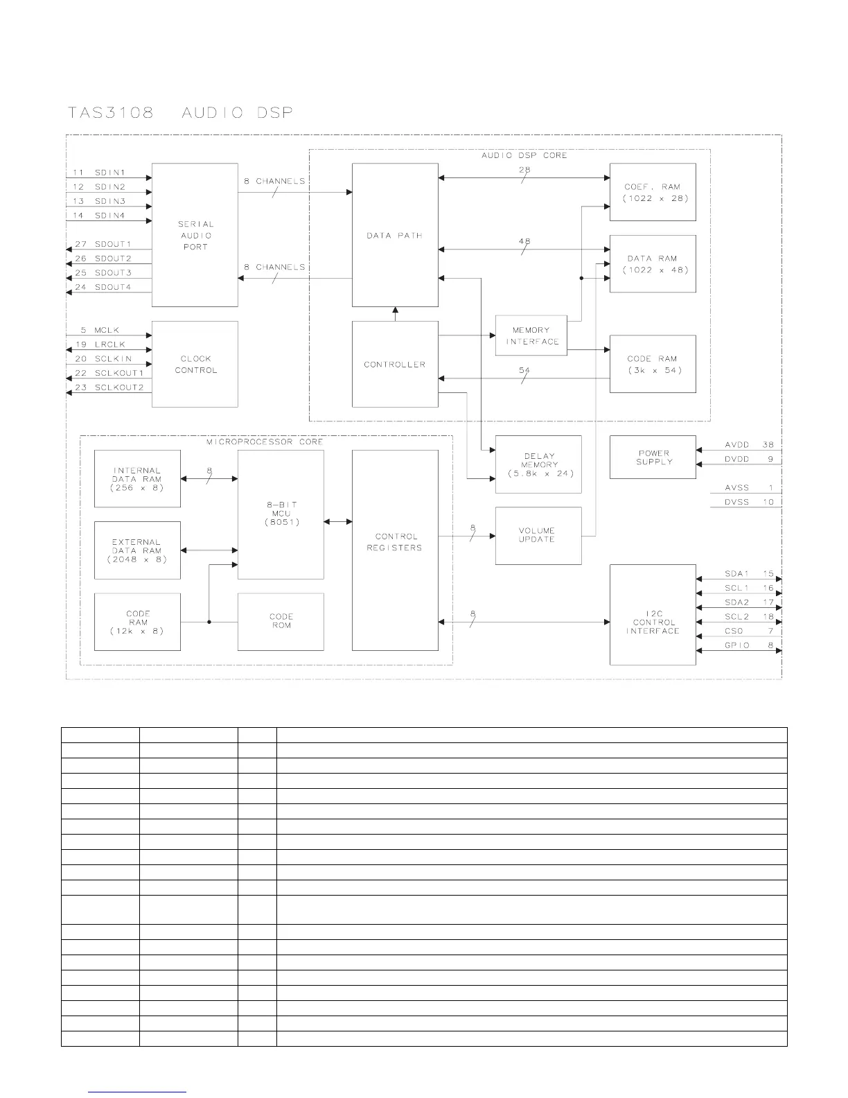
2.6. IC1403 (VHiTAS3108D-1Y)
2.6.1 Block Diagram
2.6.2 Pin Connections and short description
Pin No. Pin Name I/O Pin Function
38 AVDD — Analog power-supply input (3.3V)
1 AVSS — Analog ground
7 CS0 I Pull-down Chip select
9, 30 DVDD — Digital power-supply input (3.3V)
10, 29 DVSS — Digital ground
8 GPIO I/O Pull-up GPIO control pin (user programmable)
19 LRCLK I/O Pull-down Sample rate clock (fS) input or output
5 MCLKIN I Master clock input (Connect to ground when not in use.)
21 MCLKO O Master clock output
6 MICROCLK_DIV I Pull-down Internal microprocessor clock divide control
31 PDN I Pull-up Powers down all logic and stops all clocks, active-low. Coefficient memory remains stable
through power-down cycle.
34 PLL0 I Pull-up PLL control 0
35 PLL1 I Pull-down PLL control 1
36 PLL2 I Pull-down PLL control 2
33, 37 RESERVED — Connect to ground
32 RESET I Pull-up Reset, active-low
16 SCL1 I/O I2C port #1 clock (always a slave)
18 SCL2 I/O I2C port #2 clock (always a slave)
20 SCLKIN I Pull-down Bit clock input