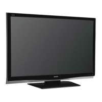
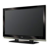
LC-42XL2E/S/RU, LC-46XL2E/S/RU, LC-46X20E/S/RU, LC-52XL2E/S/RU, LC-52X20E/S/RU
5 – 15
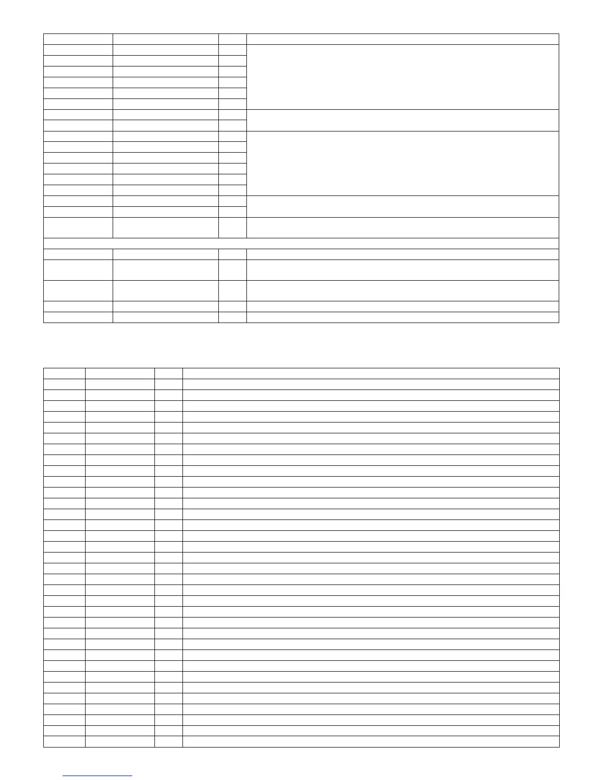
2.9. IC2002 (RH-iXB986WJN8Q)
2.9.1 Pin Connections and short description
62 R2X0+ I TMDS input Port 2 data pairs.
61 R2X0- I
65 R2X1+ I
64 R2X1- I
68 R2X2+ I
67 R2X2- I
59 R2C+ I TMDS input Port 2 clock pair.
58 R2C- I
7 TX0+ O TMDS output data pairs.
8TX0- O
4TX1+ O
5TX1- O
1TX2+ O
2TX2- O
10 TXC+ O TMDS output clock pair.
11 TXC- O
12 EXT_SWING I Voltage Swing Adjust. A resistor tied from this pin to AVCC18 determines the amplitude
of the voltage swing. The recommended value is 750Ω.
Power and Ground Pins
23, 43, 55, 63 AVCC33 — Analog VCC. Connect to 3.3V supply.
6, 17, 29, 37, 49,
57, 69
AVCC18 — Analog VCC. Connect to 1.8V supply.
3, 9, 20, 26, 40,
46, 60, 66, 80
AGND — Analog GND.
33, 73 DVCC18 — Digital VCC. Connect to 1.8V supply.
34, 74 DGND — Digital GND.
Pin No. Pin Name I/O Pin Function
1 SHIP_EN O SHIP (CSI) processing enabled/disabled selection signal
2 CS_CPLD O CPLD chip select
3 N_SRESET O Reset
4 PM_REQ O Request signal (Communication request at H)
5 IR_PASS O Remote control signal external through switching
6 Vc1 — Internal voltage drop power terminal
7 X2 I Sub clock (32.768kHz)
8 X1 O Sub clock (32.768kHz)
9 N_RESET I System reset
10 OSC2 O System clock (20.00MHz)
11 Vss — GND
12 OSC1 I System clock (20.00MHz)
13 Vcc — Power supply (+3.3V)
14 N_NMI I For FLASH rewrite
15 WAKE_UP I For WAIT mode return
16 AC_DET I For instantaneous blackout detection
17 POW_SW I Power SW
18 FRAME O Panel controller control (50/60 setting)
19 ROMSEL0 O For test pattern control
20 O_S_SET O Panel controller control ON/OFF
21 TEMP1 O Panel controller control, temperature information 1
22 TEMP2 O Panel controller control, temperature information 2
23 TEMP3 O Panel controller control, temperature information 3
24 L_R O Panel controller control, flip horizontal
25 U_D O Panel controller control, flip vertical
26 UARXD_M I Serial for MAIN CPU communication (To TXD of MAIN CPU)
27 UATXD_M O Serial for MAIN CPU communication (To RXD of MAIN CPU)
28 TXD O For debugger (E8) connection
29 RXD I For debugger (E8) connection
30 SCLD I For debugger (E8) connection
31 BUSY I For debugger (E8) connection
32 LED_R O Power LED, red
33 LED_G O Power LED, green
34 LED_OPC O OPC LED
Pin No. Pin Name I/O Pin Function