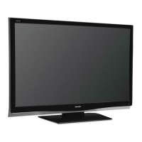
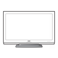
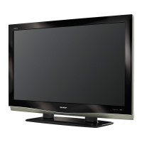
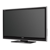
LC-42XL2E/S/RU, LC-46XL2E/S/RU, LC-46X20E/S/RU, LC-52XL2E/S/RU, LC-52X20E/S/RU
5 – 30
J3, J2, J1, H1, H2, H3, H4,
H5
TS1_D[7:0] I Transport Stream 1, data bus.
J4 TS1_DEN I Transport Stream 1, data enable.
J5 TS1_SYNC I Transport Stream 1, sync signal.
K1 TS1_CLK I Transport Stream 1, clock.
Memory Interface
AM30 DRVIMP I Driving strength impedance match reference pin.
AP29 MD0 I/O Memory data bus.
AP30 MD1 I/O Memory data bus.
AN30 MD2 I/O Memory data bus.
AN31 MD3 I/O Memory data bus.
AM33 DQM0 O Memory data write mask enable for byte 0.
AM32 DQS0 I/O Data strobe for memory data bus MD[7:0].
AL32 DQS0N I/O Data strobe for memory data bus MD[7:0].
AK30 MD4 I/O Memory data bus.
AK31 MD5 I/O Memory data bus.
AJ29 MD6 I/O Memory data bus.
AJ30 MD7 I/O Memory data bus.
AP32 MD8 I/O Memory data bus.
AP33 MD9 I/O Memory data bus.
AN33 MD10 I/O Memory data bus.
AN34 MD11 I/O Memory data bus.
AM34 DQM1 O Memory data write mask enable for byte 1.
AL33 DQS1 I/O Data strobe for memory data bus MD[15:8].
AL34 DQS1N I/O Data strobe for memory data bus MD[15:8].
AK33 MD12 I/O Memory data bus.
AK34 MD13 I/O Memory data bus.
AJ32 MD14 I/O Memory data bus.
AJ33 MD15 I/O Memory data bus.
AH33 MCLK0 O Memory clock for MD[31:0].
AH34 MCLK0N O Memory clock for MD[31:0] - active LOW.
AG29 MD16 I/O Memory data bus.
AG30 MD17 I/O Memory data bus.
AF30 MD18 I/O Memory data bus.
AF31 MD19 I/O Memory data bus.
AE33 DQM2 O Memory data write mask enable for byte 2.
AE32 DQS2 I/O Data strobe for memory data bus MD[23:16].
AD32 DQS2N I/O Data strobe for memory data bus MD[23:16].
AC30 MD20 I/O Memory data bus.
AC31 MD21 I/O Memory data bus.
AB29 MD22 I/O Memory data bus.
AB30 MD23 I/O Memory data bus.
AG32 MD24 I/O Memory data bus.
AG33 MD25 I/O Memory data bus.
AF33 MD26 I/O Memory data bus.
AF34 MD27 I/O Memory data bus.
AE34 DQM3 O Memory data write mask enable for byte 3.
AD33 DQS3 I/O Data strobe for memory data bus MD[31:24].
AD34 DQS3N I/O Data strobe for memory data bus MD[31:24].
AC33 MD28 I/O Memory data bus.
AC34 MD29 I/O Memory data bus.
AB32 MD30 I/O Memory data bus.
AB33 MD31 I/O Memory data bus.
Y33 ODT O ODT
W34 CAS O Column Access Strobe of Port A or SCAN data input.
W33 RAS O Row Access Strobe of Port A or SCAN data input.
W31 WE O Write Enable of Port A or SCAN data input.
W30 CKE O Clock enable.
V34 CS0 O Chip select for Ext Mem.
Y32 CS1 O Chip select for Ext Mem.
U33 MAA10 O Memory Address line of Port A or SCAN data input.
U32 BA1 O Internal Bank Address Select for SDRAM.
U30 BA0 O Internal Bank Address Select for SDRAM.
T34 MAA0 O Memory Address line of Port A or SCAN data output.
T31 MAA1 O Memory Address line of Port A or SCAN data output.
Ref No. Pin Name I/O Pin Function