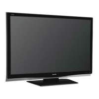
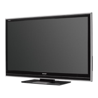
LC-42XL2E/S/RU, LC-46XL2E/S/RU, LC-46X20E/S/RU, LC-52XL2E/S/RU, LC-52X20E/S/RU
5 – 32
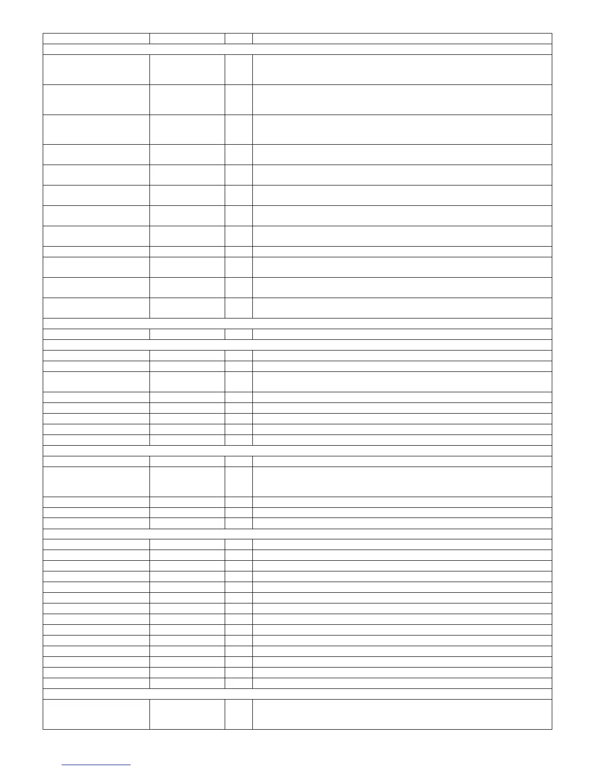
I2S Interface
T3 SCKIN O I2S: SCK of I2S input port. (Not used)
AC Link: SDATA_OUT
POD2: POD_DRXB, the second POD OOB RX data.
T4 WSI2S I I2S: WS of I2S input port. (Not used)
AC Link: ACLINK_RSTN
POD2: POD_CRXB, the second POD OOB RX gapped clock.
T5 SDI2S I I2S: SD of I2S input port. (Not used)
AC Link: SYNC
POD2: POD_QTXB, the second POD OOB TXQ channel.
U1 WS O I2S: WS of I2S output port.
AC Link: SDATA_IN_2
U2 SCK O I2S: SCK of I2S output port.
AC Link: SDATA_IN_3
U3 SD1 O I2S: SD of I2S output port.
AC Link: BIT_CLK
U4 SD2 O I2S: SD of I2S output port. (Not used)
AC Link: SDATA_IN_0
U5 SD3 O I2S: SD of I2S output port. (Not used)
AC Link: SDATA_IN_1
V5 I2SCLK O I2S: 1, 2, 4, 8 times of SCK of I2S output port, used by D/A chip.
V4 SD4 I I2S: SCK of second I2S input port. (Not used)
POD2: POD_ETXB, the second POD OOB TX enable.
V3 SD5 I I2S: WS of second I2S input port. (Not used)
POD2: POD_ITXB, the second POD OOB TXI channel.
V2 SD6 I I2S: SD of second I2S input port. (Not used)
POD2: POD_CTXB, the second POD OOB TX gapped symbol clock.
SPDIF Interface
T2 SPDIF I/O SPDIF output.
UART Interface
Y4 TXD O Data output for UART.
Y3 RTS O Request to send output for UART (8mA output pad).
Y2 DTR O Data terminal Ready output for UART (8mA output pad, 5V TTL interface 25PF, 6ns
rise timing).
Y1 RXD I Data input for UART.
AA1 CTS I Clear to send input for UART.
AA2 DSR I Data set ready for UART.
AA3 DCD I Receive line signal detect for UART. (Not used)
AA4 RI I Ring indicator for UART. (Not used)
Smart card Interface
V1 SCRST I Smart card reset 0, 8mA open-drain output pad. (Not used)
W1 SCPFET I Smart card power FET control output, 8mA open-drain output. The smart card reader
interface requires this pin to drive an external power FET to supply the current for the
Smart Card (65mA typical, 100mA short to ground). (Not used)
W2 SCIO I/O Smart card serial data, 8mA open-drain in out pad. (Not used)
W3 SCCLK O Smart card clock, 8mA open-drain output pad (7.1M to 3.5M) (Not used)
W4 SCPRES I Smart card present detect. (Not used)
CIR, RTC Interface
M1 VCCH12 — 1.2V RTC power for logic.
N1 VSSH12 — RTC ground for logic.
L1 WDOG O Watch dog reset.
L2 VCCH33 — 3.3V RTC power for logic.
L3 CK32 I 32.768 kHz crystal oscillator input.
L4 CK32E O 32.768 kHz crystal oscillator output.
L5 VSSH33 — RTC ground for logic.
M5 CRX0 I CIR0, receive data for CIRo interface.
M4 PWRON O Main power, power On control signal, low active, 4mA output pad. (Not used)
M3 PWRBT I Power switch button.
M2 VCCHRST I VCCH RST
K4 VCCH12 — 1.2V RTC power for logic.
K5 VSSH12 — RTC ground for logic.
R1 CTX0 O Transmission data for CIR interface.
Program IO
AF4 GP15 I/O Program IO.
PWM: Pulse-Width Modulation.
POD: OVERLOAD, the second POD interface current overload.
Ref No. Pin Name I/O Pin Function