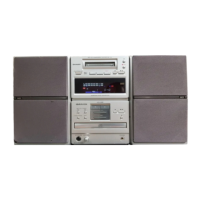
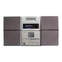
MD-X5H/CP-X5H
– 80 –
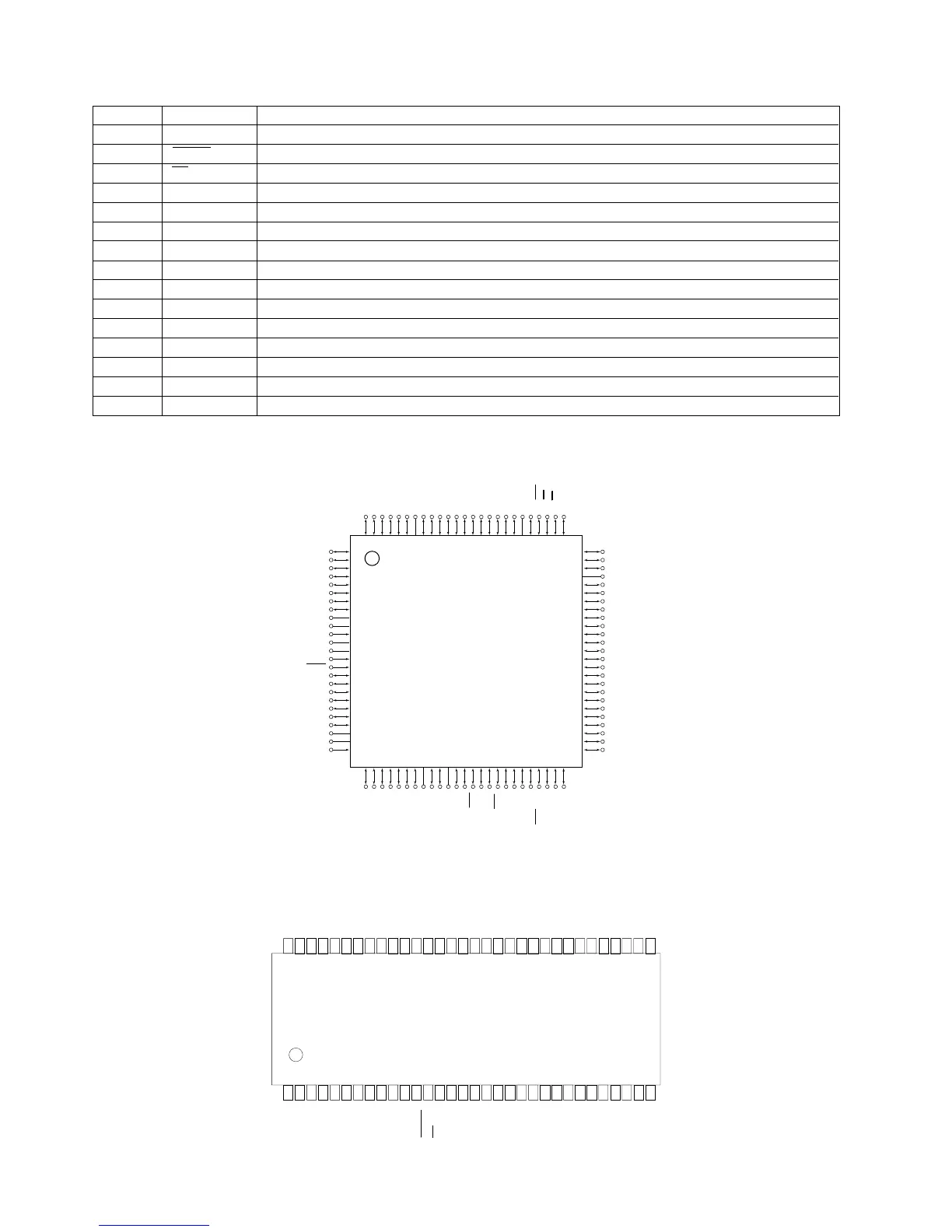
IC712 RH-iX0069AWZZ:FL Driver (IX0069AW)
1-12 DIG11-DIG00 Digit output
13 RESET Reset input
14 CS Chip selection input
15 SCK Shift clock input
16 SDATA Serial data input
17*,18* P1,P0 Output port (static operation)
19 Vcc1 Positive power terminal for internal logic
20 Xout Clock output
21 Xin Clock input
22 Vss GND terminal
23-31 SEG35-SEG27 Segment output
32 Vp Negative power terminal for VFD drive
33-59 SEG26-SEG00 Segment output
60 Vcc2 Positive power terminal for digit output and segment output
61-64 DIG15-DIG12 Digit output
Pin No.
Terminal Name
Function
In this unit, the terminal with asterisk mark (*) is (open) terminal which is not connected to the outside.
Figure 80-1 BLOCK DIAGRAM OF IC
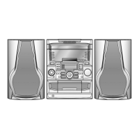
IC901 RH-iX2718AFZZ: System Control Microcomputer (iX2718AF)
IC712 RH-iX0069AWZZ: FL Driver (IX0069AW)
Figure 80-2 BLOCK DIAGRAM OF IC
1
2
3
4
5
6
7
8
9
10
11
12
13
14
15
16
17
18
19
20
21
22
23
24
25
P120/RTP0
P121/RTP1
P122/RTP2
P123/RTP3
P124/RTP4
P125/RTP5
P126/RTP6
P127/RTP7
V
DD
X2
X1
V
SS
XT2
XT1
RESET
P00/INTP0
P01/INTP1
P02/INTP2/NMI
P03/INTP3
P04/INTP4
P05/INTP5
P06/INTP6
AV
DD
AV
REF0
P10/ANI0
P11/ANI1
P12/ANI2
P13/ANI3
P14/ANI4
P15/ANI5
P16/ANI6
P17/ANI7
AV
SS
P130/ANO0
P131/ANO1
AV
REF1
P70/RxD2/SI2
P71/TxD2/SO2
P72/ASCK2/SCK2
P20/RxD1/SI1
P21/TxD1/SO1
P22/ASCK1/SCK1
P23/PCL
P24/BUZ
P25/SI0/SDA0
P26/SO0
P27/SCK0/SCL0
P80/A0
P81/A1
A82/A2
75
74
73
72
71
70
69
68
67
66
65
64
63
62
61
60
59
58
57
56
55
54
53
52
51
100 99 98 97 96 95 94 93 92 91 90 89 88 87 86 85 84 83 82 80 79 77 767881
26 27 28 29 30 31 32 33 34 35 36 37 38 39 40 41 42 43 44 46 47 49 504845
P62/A18
P61/A17
P60/A16
V
SS
P57/A15
P56/A14
P55/A13
P54/A12
P53/A11
P52/A10
P51/A9
P50/A8
P47/AD7
P46/AD6
P45/AD5
P44/AD4
P43/AD3
P42/AD2
P41/AD1
P40/AD0
P87/A7
P86/A6
P85/A5
P84/A4
P83/A3
P95
P94
P93
P92
P91
P90
TEST/V
PP
P37
P36/TI01
P35/TI00
P34/TI2
P33/TI1
P32/TO2
P31/TO1
P30/TO0
P103/TI8/TO8
P102/TI7/TO7
P101/TI6/TO6
P100/TI5/TO5
V
DD
P67/ASTB
P66/WAIT
P65/WR
P64/RD
P63/A19
IC901
IX2718AF