A
ll
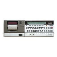
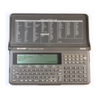
and more about Sharp P
C-
1500 at http://www.PC-1500.info
3.
LH5811
1/0
PORT
(1
I
Out
li
ne
The LH58 I
:t
l/0
port
is
the single chip I.SI of
CMOS
static circuit that can
be
connected with a
general purpose
8°
bit
CPU
.
It
has the
foUowiJlg
functions:
(I)
Two paors
of
8
-bi
t bidirectional ports
(2)
One pair
of
&.
bit
output ports
(3) Two lines
of
interrupt request inputs,
one
of
them
is
the input from
por"t.
(4) One line
of
interrupt request output.
(
5)
CPU
wait control
(
6)
Serial control
(2) Fun
ct
ions
(I
) Ports,
PAO
- PA 7 and
PBO
- PB7, can
be
programmed for l
/0
directions by each bit.
The
CPU can access
PAO
-
PA
7 and
PBO
-
PB7
as though one location
of
memory.
(2)
!'CO
-
PC7
is
the port
of
011
t
p11t
type.
The
CPU
can
acces
s
it
as
though
one
loca
t
ion
of
memory.
Also, the latch clock
P.p
to
the
PC
port can
be
supplied directly from
an
external sou
rc
e.
(3) LH58
ll
incorporates two interrupt request inputs, 1 RQ and PB7, when apply interrupt
request to the
CPU at the rising edge
of
the input when the corresponding bit
of
the internal
mask register is
"l
". Signal PB7 represents the
8th
bit
of
the port PB and it needs to be
in
the
in
put
mode when the interrupt input
is
applied.
(4) The LH5811 has a
CPU wait control circuit which uses two output lines
of
memory enable
signals for a memory that
ha
s slower access time. Jn addition, two input lines for the wait
conditions are used.
Six different
of
access times can be chosen by programming.
(5)
TI1e
following functions are provided
for
serial control.
A. Serial data transmission
Serial data transmission
is
used
in
th.e format
of
start bit/8-bit data/2 stop bits.
Transmission clock
is
programmable by changing internal and external clocks, as well as
cha11ging
the clock rate; 1/1, 1/2, 1
/128,
1
/256,
1/512, 1/1024, 1/2048, l/4096
of
the
basic clock.
B.
Seri.
al
data
re
ception
When a start bit
is
received
in
t
he
i.dle
state, 8 bits
of
data
is
received, and stored
in
the
internal register and the interrupt request
Oag
is
set
on.
Reception clock
is
sent from the external clock and must be synchronized with the
se
rial
data
input.
C.
LC
D driver control
T
he
LCD
driver is connected with three signal lines
of
the transmission clock, a serial data
bus, and a synchronous signal line to carry
out
data trans
fer
fo
r
chip
select,
addressing,
and data read/write.
For
the transmission clock in this
case
, the clock
ra
te can
be
programmed in the same
mann
er as in the serial
data
transmission clock. (Transmission clock to the
LCD
driver
is
I
MHz
.)
D.
Pul.e waveform
Th
e pul
se
waveform can be sentout
in
continuation.
Eigh
t sorts
of
frequencies arc
programmable; 1/1, 1
/2
, 1/ 128, 1
/2
56, 1/512, 1/1024, and 1/4096 Qf the basic clock.
E.
Tr3J1smiss
ion to audio casse
tt
e tape recorder
The
modulated signal can be
se
nt from the
SDO
output
in
the
fo
:miat
of
start bit/8-bit
data/2 stop
b
ih.
Modulation clocks, FX and FY, can
be
set separately to any
of
clock rate;
l/64,
l/128
,
1
/256
, 1
/512
, and
l/1024oftheba
s
ic
cl
ock.
9
Do
not sale this PDF
!!!