EasyManua.ls Logo

Sharp PC-E500S - Page 13

Sharp PC-E500S
21 pages
Print Icon
To Next Page IconTo Next Page
To Previous Page IconTo Previous Page
Loading...
@®
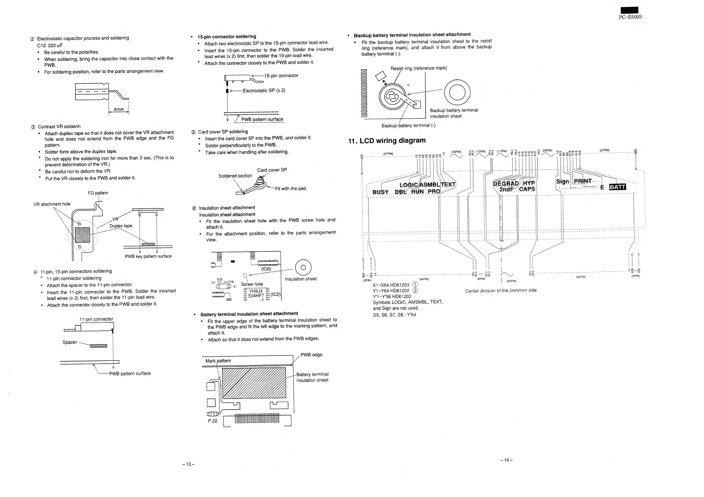
Electrostatic
capacitor
process
and
soldering
C12:
220
uF
¢
Be
careful
to
the
polarities.
|
©
When
soldering,
bring
the
capacitor
into
close
contact
with
the
PWB.
|
|
:
¢
For
soldering
position,
refer
to
the
parts
arrangement
view.
(—
-—-
—
—|
ae
aA
4mm
@
Contrast
VR
solderin
*
Attach
duplex
tape
so
that
it
does
not
cover
the
VR
attachment
hole
and
does
not
extend
from
the
PWB
edge
and
the
FG
pattern.
¢
Solder
form
above
the
duplex
tape.
*
Do
not
apply
the
soldering
iron
for
more
than
3
sec.
(This
is
to
prevent
deformation
of
the
VR.)
Be
careful
not
to
deform
the
VR.
*
Put
the
VR
closely
to
the
PWB
and
solder
it.
FG
‘ial
VR
attachment
hole
peateeta
VR
ae
7
_
Duplex
tape
or
|
PWB
key
pattern
surface
@
11-pin,
15-pin
connectors
soldering
*
41-pin
connector
soldering
e
Attach
the
spacer
to
the
11-pin
connector.
¢
insert
the
11-pin
connector
to
the
PWB.
Solder
the
inserted
lead
wires
(x
2)
first,
then
solder
the
11-pin
lead
wire.
*
Attach
the
connector
closely
to
the
PWB
and
solder
it.
11-pin
connector
Spacer
Vv
PWB
pattern
surface
15-pin
connector
soldering
*
Attach
two
electrostatic
SP
to
the
15-pin
connector
lead
wire.
¢
Insert
the
15-pin
connector
to
the
PWB.
Solder
the
inserted
lead
wires
(x
2)
first,
then
solder
the
15-pin
lead
wire.
*
Attach
the
connector
closely
to
the
PWB
and
solder
it.
<———{5-pin
connector
<——-
Electrostatic
SP
(x
2)
PWEB
pattern
surface
Card
cover
SP
soldering
*
Insert
the
card
cover
SP
into
the
PWB,
and
solder
it.
*
Solder
perpendicularly
to
the
PWB.
*
Take
care
when
handling
after
soldering.
Card
cover
SP
-
Soldered
section
S—
Fit
with
the
pad.
©
Insulation
sheet
attachment
SF
Insulation
sheet
attachment
¢
Fit
the
insulation
sheet
hole
with
the
PWB
screw
hole
and
attach
it.
¢
For
the
attachment
position,
refer
to
the
parts
arrangement
view.
C15
Insulation
sheet
2a,
Sa
O16
X1
EVHILH
=
cmon?
|
=
834HF7
=
(IC2)
a
\
Screw
hole
Battery
terminal
insulation
sheet
attachment
¢
Fit
the
upper
edge
of
the
battery
terminal
insulation
sheet
to
the
PWB
edge
and
fit
the
left
edge
to
the
marking
pattern,
and
attach
it.
°
Attach
so
that
it
does
not
extend
from
the
PWB
edges.
PWB
edge
Mark
pattern
Battery
terminal
insulation
sheet
¢
Backup
battery
terminal
insulation
sheet
attachment
e
Fit
the
backup
battery
terminal
insulation
sheet
to
the
resist
ring
(reference
mark),
and
attach
it
from
above
the
backup
battery
terminal
(-).
AMUN
UNA
Resist
ring
(reference
mark)
e.
Backup
battery
terminal
insulation
sheet
Backup
battery
terminal
(-)
11.
LCD
wiring
diagram
--
OLX
eeoe
-
a
i)
~
(27P1N)
eet
ea
eS
ee,
SS
eo
Se
Sie
ee
ee
“SS
SUS)
Seis
eS
a
eee
=
wie
ee!
ae
eee
aie
leet
ea
a
eke
ole
et
et
ee
eee
ee
eee
Ss
Susi
<<
_
<<
ete
ae:
ee
Soars
Ge
Sera)
fe
2
Seay
eerie
Se
eo)
Seite)
6)
SS
tO
(Se
See
eee
Se
me
ees
Vs
~~
WA
oO
COO
(64PIN)
(8PIN)
a
|
(20PIN)
X1~X64
HD61203
(1)
Y1~Y64
HD61202
(2)
Y'1~¥'56
HD61202
Symbols
LOGIC,
AMSMBL,
TEXT,
and
Sign
are
not
used.
$5,
S6,
S7,
S8:
Y'64
a,
7
(12PIN)
SX
(11PIN)
<<
GB
\_)
B
Center
division
of
the
common
side
(27PIN)
PC-E5005
Sigel
wl
me
ee
ee
ce
tase
ee