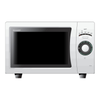
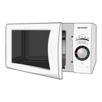
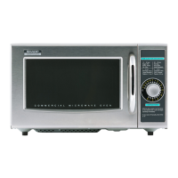
16
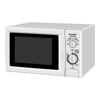
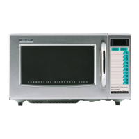
R-216(G)
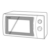
R-216(IN)
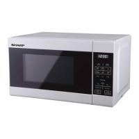
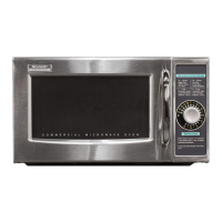
R-216(W)
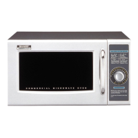
R-216(Y)
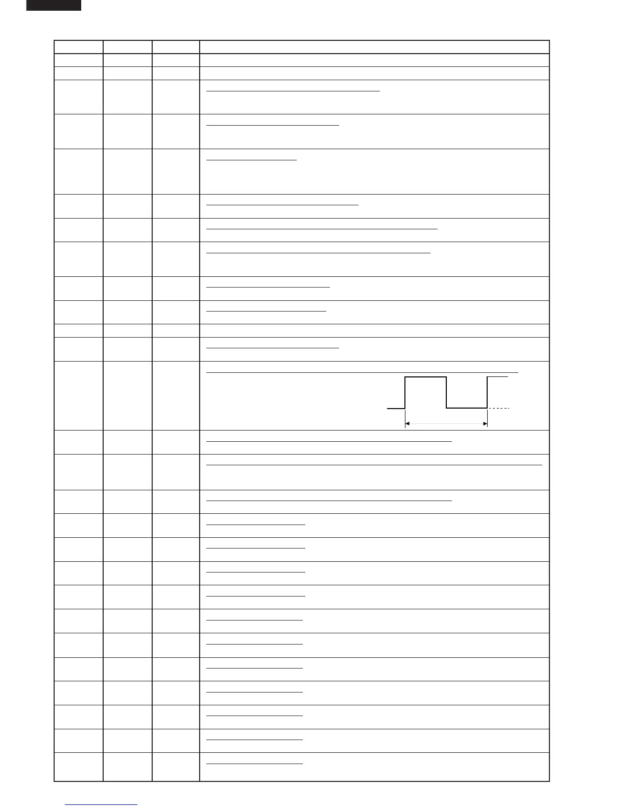
Pin No. Signal I/O Description
5D7IN/OUT Terminal not used.
6 P20 IN Connected to 0V.
7 P21 IN Signal coming from touch tact switch.
When tact switch SW2 is touched, a signal will be input into P21. When tact switch
is not touched, the signal is held at “H” level.
8 P22 IN Signal coming from encoder.
When the encoder is turned, the contacts of encoder make pulse signals. And
pulse signals are input into P22.
9 RESET IN Auto clear terminal.
Signal is input to reset the LSI to the initial state when power is applied. Temporarily
set to “L” level the moment power is applied, at this time the LSI is reset. Thereafter
set at “H” level.
10 CNVSS IN Reference voltage input terminal.
A reference voltage is applied to the A/D converter in the LSI. Connected to VC.
11 XOUT OUT Internal clock oscillation frequency control output.
Output to control oscillation input of XIN.
12 XIN IN Internal clock oscillation frequency input setting.
The internal clock frequency is set by inserting the ceramic filter oscillation circuit
with respect to XOUT terminal.
13 VSS IN Power source voltage: -5V.
The power source voltage to drive the LSI is input to VSS terminal. Connected to VC.
14 VDD IN Power source voltage: 0V.
The power source voltage to drive the LSI is input to VDD terminal.
15 N.F IN Connected to VSS terminal.
16 INT0 IN Signal coming from encoder.
Signal similar to INT0. Pulse signals are input into INT0.
17 INT1 IN Signal to synchronize LSI with commercial power source frequency.
This is basic timing for all real time
processing of LSI.
18-19 AIN0-AIN1 IN Terminal to change functions according to the model.
Signal in accordance with the model in operation is applied to set up its function.
20 AIN2 IN Input signal which communicates the door open/close information to LSI.
Door closed; “H” level signal.
Door opened; “L” level signal.
21 AIN3 IN Terminal to change functions according to the model.
Signal in accordance with the model in operation is applied to set up its function.
22 P00 OUT Digit selection signal.
Signal is input to the anodes of the light-emitting diodes (LD30 - LD34).
23 P01 OUT Digit selection signal.
Signal is input to the anodes of the light-emitting diodes (LD9 - LD16).
24 P02 OUT Digit selection signal.
Signal is input to the anodes of the light-emitting diodes (LD17 - LD24).
25 P03 OUT Digit selection signal.
Signal is input to the anodes of the light-emitting diodes (LD1 - LD8).
26 P10 OUT Segment data signal.
Signal is input to the cathodes of the light-emitting diodes (LD1, LD9, LD17 and LD30).
27 P11 OUT Segment data signal.
Signal is input to the cathodes of the light-emitting diodes (LD2, LD10, LD18 and LD31).
28 P12 OUT Segment data signal.
Signal is input to the cathodes of the light-emitting diodes (LD3, LD11, LD19 and LD32).
29 P13 OUT Segment data signal.
Signal is input to the cathodes of the light-emitting diodes (LD4, LD12 and LD20).
30 D0 OUT Segment data signal.
Signal is input to the cathodes of the light-emitting diodes (LD5, LD13, LD21 and LD33).
31 D1 OUT Segment data signal.
Signal is input to the cathodes of the light-emitting diodes (LD6, LD14, LD22 and LD34).
32 D2 OUT Segment data signal.
Signal is input to the cathodes of the light-emitting diodes (LD7, LD15 and LD23).
20 msec
H : GND
L (-5V)