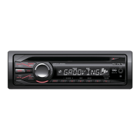
CDX-GT24W/GT240/GT290/GT290S
CDX-GT24W/GT240/GT290/GT290S
1818
4-2. BLOCK DIAGRAM – DISPLAY Section –
For Schematic Diagrams.
Note:
• All capacitors are in μF unless otherwise noted. (p: pF) 50
WV or less are not indicated except for electrolytics and
tantalums.
• All resistors are in Ω and 1/4 W or less unless otherwise
specifi ed.
•
f
: Internal component.
• C : Panel designation.
THIS NOTE IS COMMON FOR PRINTED WIRING BOARDS AND SCHEMATIC DIAGRAMS.
(In addition to this, the necessary note is printed in each block.)
• A : B+ Line.
• B : B– Line.
• Voltages and waveforms are dc with respect to ground
under no-signal (detuned) conditions.
no mark
: FM
( ) : AM/MW/SW
< > : CD PLAY
• Voltages are taken with VOM (Input impedance 10 MΩ).
Voltage variations may be noted due to normal production
tolerances.
• Waveforms are taken with a oscilloscope.
Voltage variations may be noted due to normal production
tolerances.
• Circled numbers refer to waveforms.
• Signal path.
J : CD PLAY
F : FM
f : AM/MW/SW
L : AUX
• Abbreviation
CND : Canadian model
AR : Argentine model
EA : Saudi Arabia model
MX : Mexican model
For Printed Wiring Boards.
Note:
• X : Parts extracted from the component side.
•
a
: Through hole.
• : Pattern from the side which enables seeing.
(The other layers’ patterns are not indicated.)
• Indication of transistor.
C
B
These are omitted.
E
Q
Caution:
Pattern face side:
(SIDE B)
Parts face side:
(SIDE A)
Parts on the pattern face side seen
from the pattern face are indicated.
Parts on the parts face side seen from
the parts face are indicated.
Note:
The components identi-
fi ed by mark 0 or dotted
line with mark 0 are criti-
cal for safety.
Replace only with part
number specifi ed.
Note:
Les composants identifi és
par une marque 0 sont
critiques pour la sécurité.
Ne les remplacer que par
une pièce portant le nu-
méro spécifi é.
• Waveforms
– MAIN Board –
40 mVp-p
4 MHz
1.7 Vp-p
32.768 kHz
20 mV/DIV, 100 nsec/DIV
0.5 V/DIV, 10 Psec/DIV
1 IC1 qh (XTAL1)
2 IC501 qa (XOUT)
3.4 Vp-p
11.06 MHz
1 V/DIV, 50 nsec/DIV
3 IC501 qd (OSCOUT)
• Abbreviation
CND : Canadian model
AR : Argentine model
EA : Saudi Arabia model
MX : Mexican model
X502
32.768kHz
10
11
94
1
2
100
95
SYSTEM CONTROL
IC501 (2/2)
LCD DRIVE
IC903
KEYIN1
CL
CE
LCD_SO
LCD_CKO
LCD_CE
DIMMER
KEYIN0
92
KEYACK1
82
RE-IN0
RE-0
RE-1
81
RE-IN1
42
RC_IN1
97
RC_IN0
91
KEYACK0
XOUT
XIN
X501
11.06MHz
15
13
OSCOUT
3
NOSE_SW
OSCIN
47
48
46
2
COM1
I
COM4
LCD901
LIQUID
CRYSTAL
DISPLAY
PANEL
3
I
34
39
35
|
38
S1
I
S33
DI
DIMMER
SWITCH
Q931
LED931
PANEL+B
()
KEY MATRIX
LSW902–908,
S901–907
(VOLUME)
PUSH SELECT
S909
ROTARY
ENCODER
BACK LIGHT
1
LCD
BACK LIGHT
SWITCH
Q932
LCD BACK
LIGHT
()
LED901,903,905,908,
910,911,913,916,918,
919,921,923,925,927,
LSW902–908
KEY
ILLUMINATE
4
SIRCS
70
AREASEL2
10K
9K
S502
FREQUENCY
SELECTOR
BU+3.3V
E,AR,MX MODEL
GT290/GT290S
J561
(REMOTE IN)
REMOTE
CONTROL
SIGNAL
RECEIVER
IC902
x Abbreviation
AR : Argentine model
MX : Mexican model
Ver. 1.1

 Loading...