Great user manuals database on UserManuals.info
38
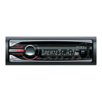
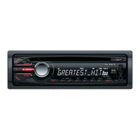
CDX-GT50W/GT500/GT500EE/GT550
IC711 MB90487APF-G-162E1 (SYSTEM CONTROL) (MAIN BOARD (3/3))
Pin No. Pin Name I/O Pin Description
1 AREASEL2 I Destination setting pin
2 AREASEL1 I Destination setting pin
3 AREASEL0 I Destination setting pin
4 NCO O Not used. (Open)
5 NOSE SW I Front panel open/close detect signal input L: Panel on, H: Panel off
6 NCO O Not used. (Open)
7 BEEP O Beep signal output
8 DIAG I Power AMP status signal input
9 VOL ATT O Electronic volume attenuate control signal output
10 FSW IN I D/D converter oscillater frequency count signal input
11 VSS — Ground pin
12 TUATT O Tuner mute control signal output
13 NSMASK O Noise mask signal output (AEP, UK model only)
14 ILLUMI SEL I Illumination voltage setting signal input
15 SEL1 O Not used in this set. (Open)
16 NCO O Not used. (Open)
17 AUXIN O AUX select signal output L: AUX, H: BUS IN
18 DISP RSET O Display reset signal output
19 FL ON O D/D converter control signal output H: On
20 DISP ON O Display control signal output H: On
21 ATT O Audio mute control signal output
22 SYSRST O System control reset signal output
23 VCC5 — Power supply pin (+3.3 V)
24 EEP SIO I/O EEPROM bus serial data input/output
25 EEP CKO O EEPROM bus serial clock output
26 AMPSTB O Power AMP satandby signal output
27 DISP RX I/O Display IC communication signal input/output
28 DISP TX O Display IC communication signal output
29 MAST IF O Display IC communication start signal output
30 RDS ON O RDS ON signal output (AEP, UK model only)
31 RE IN0 I Rotary encoder signal input 0
32 RE IN1 I Rotary encoder signal input 1
33 I2C SCK O I2C bus serial clock signal output
34 I2C SIO I/O I2C bus serial data signal input/output
35 DAVDD — A/D converter power supply pin (+3.3 V)
36 AVRH — A/D converter external reference power supply pin (+3.3 V)
37 DAVSS — Ground pin
38 QUALITY I Noise detect signal input (AEP, UK model only)
39 VSM I S-meter voltage detect signal input
40 KEYIN1 I Key signal input 1
41 KEYIN0 I Key signal input 0
42 VSS — Ground pin
43 RC IN0 I Rotary commander key signal input
44 SA IN I Spectrum analyzer signal input
45 SA CKO O Spectrum analyzer clock signal output
46 to 48 NCO O Not used. (open)
49 MD0 I Operation mode setting pin (Connect to VDD.)
50 MD1 I Operation mode setting pin (Connect to VDD.)
51 MD2 I Operation mode setting pin (Connect to VSS.)
 Loading...