34
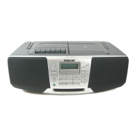
CFD-S01
• IC PIN DESCRIPTIONS
• IC701 BU9532KS2 (RF AMP, SYSTEM SERVO PROCESSOR, DIGITAL SIGNAL PROCESSOR) (MAIN BOARD (1/4))
Pin No. Pin Name I/O Pin Description
1AVDD1 I Power supply pin (+3.3V)
2AC (I) I A+C RF signal input
3 BD (I) I B+D RF signal input
4 VBIAS (O) O VC voltage output
5E (I) I E RF signal input
6F (I) I F RF signal input
7 PKC (O) O RF signal peak detector capacitor fitted
8 FEN (I) I Focus error amp input
9 FEO (O) O Focus error output
10 BTC (O) O RF signal bottom detector capacitor fitted
11 PD (I) I Photo detector signal input
12 LD (O) O Laser diode drive signal outout
13 ASY (I) I Asymmentric correction input
14 PCO (O) O PLL PCO output
15 FCO (O) O PLL FCO-DAC output
16 AGND1 — Ground
17 FDOUT (O) O Focus drive signal output
18 JUMPO (O) O track jump pulse drive signal input
19 TDOUT (O) O Tracking drive sigmal outout
20 SDIN (I) I Sled drive signal input
21 SDOUT (O) O Sled drive signal output
22 CLVOUT (O) O CLV drive signal output
23 CLK88 (O) O Not used (Open)
24 LON (O) O Not used (Open)
25 CLK (O) O Not used (Open)
26 SUBSYQ (O) O Sub code synchronous signal output
27 MCK (I) I Command transfer clock input
28 DIN (I) I Status and SUB-Q data input
29 DOUT (O) O Command data output
30 R/W (I) I Command read/write signal input
31 RESETX (I) I Reset signal input
32 BUSY (O) O BUSY signal output
33 MONI 0 I Test input (Not used (pull duwn))
34 MONI 1 I Muting signal input
35 XPCLK O XPCLK signal output
36 DVDD — Power supply pin (+3.3V)
37 XI (I) I Main clock input (18.432MHz)
38 XO (O) O Main clock output (18.432MHz)
39 DGND — Ground
40 AVDD2 — Power supply pin (+3.3V)
41 LDACO (O) O Audio L-CH output
42 VCDAC O Audio DAC reference voltage output
43 RDACO (O) O Audio R-CH output
44 AGND2 — Ground
45 RFRPRFM (O) O RFRP capacitor fitted
46 TZCRFM (O) O TZC capacitor fitted
47 SC (O) O Scratch depth ajstment output
48 TEO (O) O Tracking error outpot