35
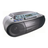
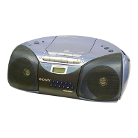
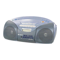
CFD-S03CP/S03CPL
48 AVDD0 — Power supply terminal (+3.3V)
49 AVSS0 — Ground terminal
50 E I E signal input from the optical pick-up block
51 F I F signal input from the optical pick-up block
52 TEI I Tracking error signal input terminal
53 TEO O Tracking error signal output terminal
54 FEI I Focus error signal input terminal
55 FEO O Focus error signal output terminal
56 VC O Middle point voltage output terminal
57 A I A signal input from the optical pick-up block
58 B I B signal input from the optical pick-up block
59 C I C signal input from the optical pick-up block
60 D I D signal input from the optical pick-up block
61 AVDD4 — Power supply terminal (+3.3V)
62 RFDCO O Not used
63 PDSENS I Not used
64 AC_SUM O RFAC summing amplifier signal output terminal
65 EQ_IN I RF equalizer circuit input terminal
66 LD O
Laser diode on/off control signal output to the automatic power control circuit
“L”: laser off, “H”: laser on
67 PD I Light amount monitor input from the optical pick-up block laser diode
68 RFC I Equalizer cut off frequency adjustment terminal
69 AVSS4 — Ground terminal
70 RFACO O EFM signal output terminal
71 RFACI I EFM signal input terminal
72 AVDD3 — Power supply terminal (+3.3V)
73 BIAS I Asymmetry circuit constant current input terminal
74 ASYI I Playback EFM asymmetry comparator voltage input terminal
75 ASYO O Playback EFM full-swing output terminal
76 VPCO O Charge pump output terminal for broad-band EFM PLL
77 VCTL I VCO2 control voltage input terminal for broad-band EFM PLL
78 AVSS3 — Ground terminal
79 CLTV I VCO1 control voltage input terminal for multiplier
80 FILO O Filter output terminal for master PLL
81 FILI I Filter input terminal for master PLL
82 PCO O Charge pump output terminal for master PLL
83 SVSS — Ground terminal
84 SVDD — Power supply terminal (+1.8V)
85 SSTB-MP3 I MP3 standby on/off control signal input terminal “L”: standby Not used
86 VDD — Power supply terminal (+1.8V)
87 VSS — Ground terminal
88 TEST1 I Test terminal Normally: fixed at “L”
89 DATA I CD serial data input from the system controller
90 CLK2 I MP3 serial data transfer clock signal input from the system controller
91 SVSS — Ground terminal
92 SVDD — Power supply terminal (+2.5V)
93 JTAGTCK — Not used
94 JTAGTDI — Not used
95 JTAGTDO — Not used
96 JTAGTMS — Not used
Pin No. Pin Name I/O Pin Description