1
A
B
C
D
E
F
G
H
234 5
04
CNP1 CNP2
C97
(11)
1
A
B
C
D
E
F
G
H
234567
04
(11)
(TEST A)
TAPE
(TEST B)
·
ª
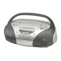
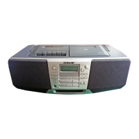
CFD-S39
– 25 –
6-6. PRINTED WIRING BOARD — TUNER SECTION — • Refer to page 17 for Circuit Boards Location.
– 26 –
Note:
• X : parts extracted from the component side.
•
¢
: internal component.
• b : Pattern from the side which enables seeing.
6-7. PRINTED WIRING BOARD — CONTROL SECTION — • Refer to page 17 for Circuit Boards Location.
Note:
• X : parts extracted from the component side.
• b : Pattern from the side which enables seeing.
(Page 28) (Page 28)
(Page 28)
D601 D-3
D602 E-3
D603 F-3
D604 F-4
D605 G-4
IC601 C-3
Ref. No. Location
• Semiconductor
Location
(control board)
D1 E-5
D2 D-4
D3 B-4
D5 G-5
D6 H-5
D7 H-5
D10 B-1
D11 B-1
IC1 F-4
IC2 F-1
Q12 D-3
Q13 D-2
• Semiconductor
Location
(tuner board)
Ref. No. Location

 Loading...