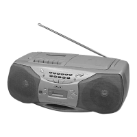
CFD-S39
– 29 –
6-9. SCHEMATIC DIAGRAM — MAIN SECTION (1/3) — • Refer to page 41 for IC Block Diagrams.
– 30 –
Note on Printed Wiring Boards:
• X : parts extracted from the component side.
• b : Pattern from the side which enables seeing.
Note on Schematic Diagram:
• All capacitors are in µF unless otherwise noted. pF: µµF
50 WV or less are not indicated except for electrolytics
and tantalums.
• All resistors are in Ω and
1
/
4
W or less unless otherwise
specified.
• C : panel designation.
• U : B+ Line.
• Power voltage is dc 9 V and fed with regulated dc power
supply from battery terminal.
• Voltage and waveforms are dc with respect to ground
under no-signal (detuned) conditions.
no mark : TAPE PB
( ) : TAPE REC
• Voltages are taken with a VOM (Input impedance 10 MΩ).
Voltage variations may be noted due to normal produc-
tion tolerances.
• Signal path.
F : FM
E : TAPE PB
a : TAPE REC
(Page 38)
(Page 32)
(Page 24)
(Page 33)
Ref. No. Location
D302 C-5
D303 H-5
D351 D-3
D501 E-6
D502 E-7
D590 D-7
D591 E-7
D951 H-5
D952 H-5
D953 I-4
D955 H-5
D957 I-5
IC301 F-5
IC303 I-7
IC304 I-8
• Semiconductor Location
Ref. No. Location
IC501 C-8
IC502 D-6
IC503 B-10
IC701 H-13
IC702 H-11
IC703 E-13
Q301 C-5
Q311 F-9
Q312 F-10
Q313 G-10
Q321 C-6
Q322 C-5
Q323 C-5
Q324 C-5
Q325 C-4
Ref. No. Location
Q326 C-5
Q501 D-8
Q502 D-8
Q503 C-12
Q505 B-10
Q506 B-10
Q701 I-12
Q951 G-4
Q952 H-4
Q953 I-4
Q954 H-4
Q955 I-4
Q957 I-5
Q958 E-4
Q959 E-4
Q960 D-5
(Page 39)