15
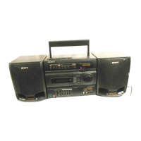
CFM-D1JMK2/D1MK2
• IC BLOCK DIAGRAMS
IC101 MM1315AS
For schematic diagrams.
Note:
• All capacitors are in µF unless otherwise noted. pF: µµF 50 WV
or less are not indicated except for electrolytics and tantalums.
• All resistors are in Ω and
1
/
4
W or less unless otherwise specified.
•
¢
: internal component.
For printed wiring boards.
Note:
• ¢ : internal component.
• : Pattern from the side which enables seeing.
• Abbreviation
EA : Saudi Arabia
UAE : United Arab Emirates
SP : Singapore
Note : The components identified by mark ! or dotted
line with mark ! are critical for safety.
Replace only with part number specified.
• U : B+ Line
•Voltages are dc with respect to ground under no-signal(detuned)
conditions.
no mark : FM
( ) : MW
<>: REC
[]: PLAY
• Voltages are taken with a VOM (10MΩ/V).
Voltage variations may be noted due to normal production tolerances.
• Signal path.
F : FM
E : PB
G : REC
f : MW
• Abbreviation
EA : Saudi Arabia
UAE : United Arab Emirates
SP : Singapore