CFS-616S
– 21 – – 22 – – 23 –
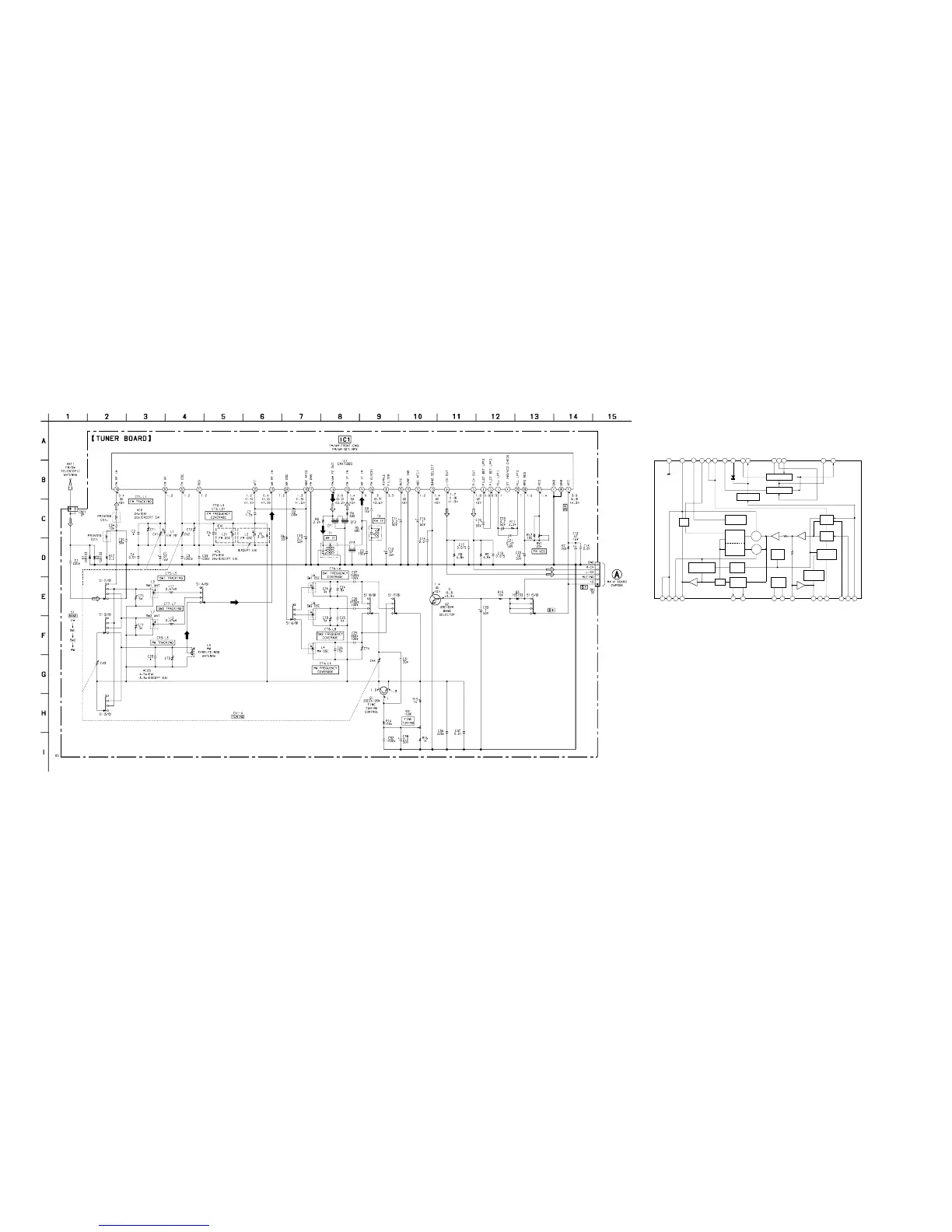
6-4. SCHEMATIC DIAGRAM – TUNER Section –
Note on Schematic Diagram:
• All capacitors are in µF unless otherwise noted. pF: µµF
50 WV or less are not indicated except for electrolytics
and tantalums.
• All resistors are in Ω and
1
/4
W or less unless otherwise
specified.
•
¢
: internal component.
• C : panel designation.
• U : B+ Line.
• H : adjustment for repair.
• Power voltage is dc 9V and fed with regulated dc power
supply from battery terminal.
• Voltages are dc with respect to ground under no-signal
(detuned) conditions.
no mark : FM
( ) : MW
< > : SW
• Voltages are taken with a VOM (Input impedance 10 MΩ).
Voltage variations may be noted due to normal produc-
tion tolerances.
• Signal path.
F: FM/SW
f: MW
• Abbreviation
EA: Saudi Arabia model.
VCO
REGULATOR
FM FRONT-END
AM FRONT-END
MPX
REGULATOR
MONO/STEREO
SELECT
DECORD
AMP
MUTING
AUTO
BLEND
TUNING
INDICATOR
AM IF/
DET
FM IF/
DISCRI
RIPPLE
FILTER
BAND-PASS
MUTE
1
27
28
2930 242526 212223 181920 1617
2 3 4 5 6 7 8 9
PLL LPF1
PILOT DET LPF2
PILOT DET LPF2
ST IND/VCO CHECK
L-CH OUT
VCC
R-CH OUT
RIPPLE FILTER
AGC AFC1
10
AGC AFC2
13
FM IF IN
14
AM IF IN
15
BAND SELECT
11
GND
12
TUNE IND
1/2
COUNTER
1/2
COUNTER
PD1
PD2
FM/AM FE OUT
FM GND
FM RF IN
AM RF IN
FM RF
REG
FM OSC
AFC
AM OSC
MUTE
FM DISCRI
GND
PLL LPF2
MPX REG
VCO
• IC Block Diagram
IC1 CXA1238S