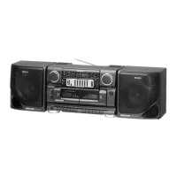
CFS-616S
– 27 – – 28 – – 29 – – 30 –
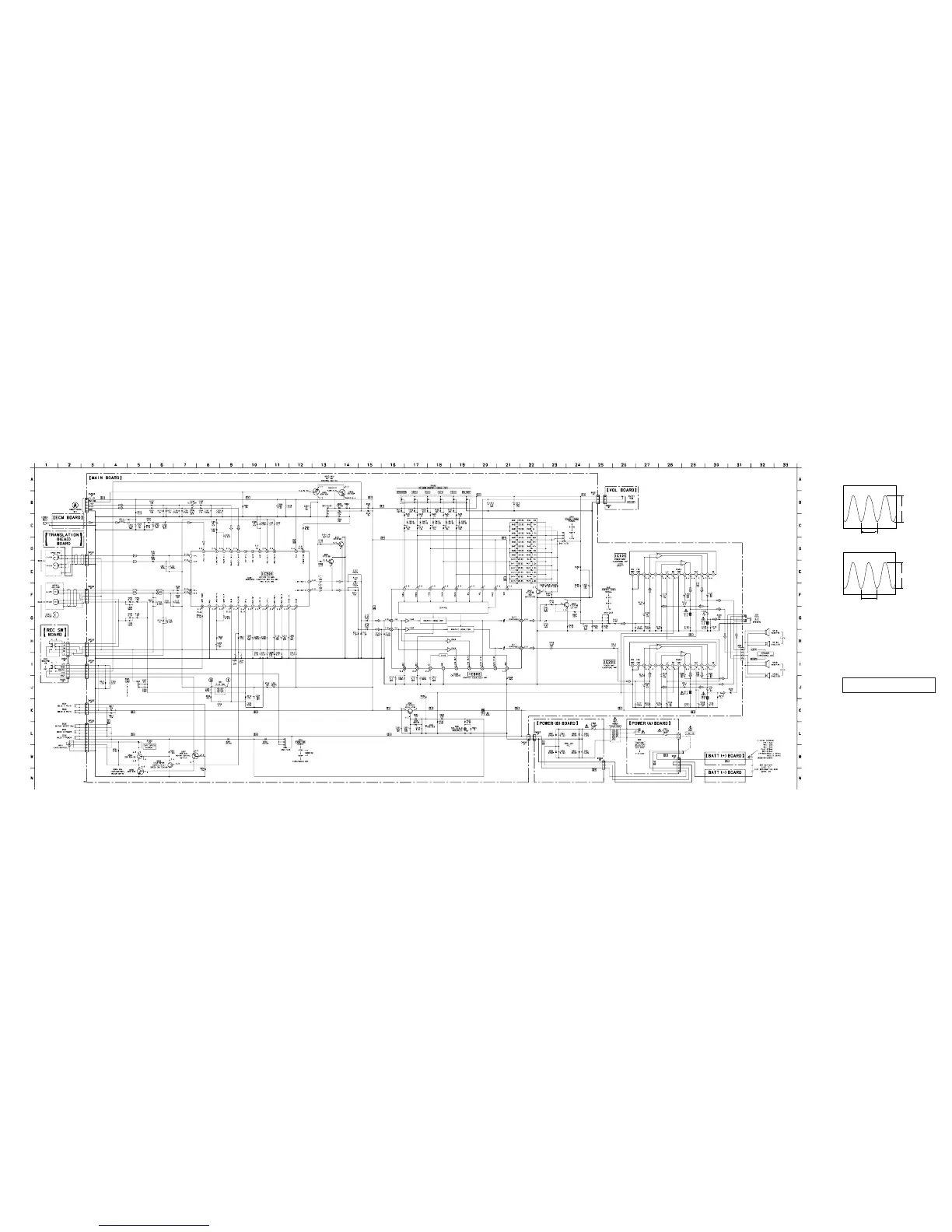
6-6. SCHEMATIC DIAGRAM – MAIN Section – • See page 31 for IC Block Diagrams.
Note on Schematic Diagram:
• All capacitors are in µF unless otherwise noted. pF: µµF
50 WV or less are not indicated except for electrolytics
and tantalums.
• All resistors are in Ω and
1
/4
W or less unless otherwise
specified.
• C : panel designation.
• U : B+ Line.
• H : adjustment for repair.
• Power voltage is dc 9 V and fed with regulated dc power
supply from battery terminal.
• Voltages and waveforms are dc with respect to ground
under no-signal conditions.
no mark : TAPE PLAY
( ) : TAPE REC
• Voltages are taken with a VOM (Input impedance 10 MΩ).
Voltage variations may be noted due to normal produc-
tion tolerances.
• Waveforms are taken with a oscilloscope.
Voltage variations may be noted due to normal produc-
tion tolerances.
• Circled numbers refer to waveforms.
• Signal path.
F : TUNER
E : TAPE PLAY (DECK A)
d : TAPE PLAY (DECK B)
G : TAPE REC (DECK B)
N : MIC INPUT
Note: The components identified by mark ! or dotted line
with mark ! are critical for safety.
Replace only with part number specified.
• Waveforms
– MAIN Board –
1 T301 (REC mode)
10V/DIV, 5 µs/DIV
2 T301 (REC mode)
1V/DIV, 5 µs/DIV
 Loading...