F
Felicia JarvisSep 12, 2025
Why does my Sony Cyber-shot DSC-P1 record incorrect date and time?
- AAnnette HarrisSep 12, 2025
If the date and time are recorded incorrectly on your Sony Digital Camera, set the correct date and time.
Why does my Sony Cyber-shot DSC-P1 record incorrect date and time?
If the date and time are recorded incorrectly on your Sony Digital Camera, set the correct date and time.
Why does my Sony Cyber-shot DSC-P1 cannot delete an image?
If your Sony Digital Camera is unable to delete an image, cancel the protection setting.
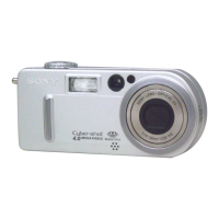
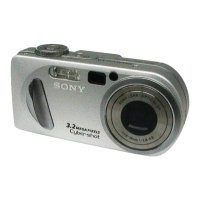
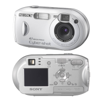
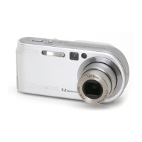
| Image Resolution | 2048 x 1536 |
|---|---|
| Digital Zoom | 2x |
| Display | LCD |
| Screen size | 1.5 inches |
| Storage Media | Memory Stick |
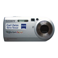
| Lens | Carl Zeiss Vario-Tessar |
| Maximum Aperture | F2.8 |
| Aperture | f/2.8 - f/5.6 |
| ISO Sensitivity | 100, 200 |
| Battery | InfoLithium |
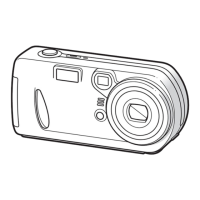
Details and diagrams for identifying the various external components of the camera.
Essential warnings and guidelines for safe operation, storage, and handling of the camera.
Covers FCC, EMC directives, and other compliance standards applicable to the device.
Provides a visual guide and sequence for the camera's disassembly process.
Procedure for replacing the BT lid assembly, noting variations based on model code.
Details for replacing the rear cabinet block, PD-137 board, and ZM-26 board.
Procedures for replacing the SW-349 board and the LCD module.
Method for replacing the rear aluminum cabinet assembly and related parts.
Procedure for replacing the rear inner cabinet assembly and associated components.
Instructions for replacing the camera's jack cover.
Procedures for disassembling the upper cabinet, PW-122 board, and lens block.
Details for replacing the CA-66 and PS-440 circuit boards.
Procedures for replacing DD-150, ST-62, HI-74, and MT-60 circuit boards.
Diagrams illustrating the physical placement of all major circuit boards within the camera.
Provides a high-level overview of the camera's main functional blocks and their interconnections.
Detailed schematic of the camera's power supply system, part 1.
Overall schematic diagrams showing the frame and major board interconnections.
Printed wiring board and schematic for the CCD imager module.
Illustrations and descriptions of key signal waveforms for diagnostic purposes.
Diagrams indicating the physical location of components on various circuit boards.
Procedure to safely discharge the high-voltage capacitor in the flashlight circuit before adjustments.
Procedure for adjusting the lens flange back distance for optimal focus.
Procedure for inputting initial data into the LCD system for proper display function.
Instructions for operating the remote commander for calibration and data setting.
Diagrams showing the assembly and part numbers for the upper cabinet section.
Diagrams showing the assembly and part numbers for the rear panel section.
Diagrams showing the assembly and part numbers for the main camera section.
Detailed list of electrical components for the PD-137 board, including part numbers and specifications.