D-NF430/NF431
2020
D-NF430/NF431
• Waveforms
– MAIN Board –
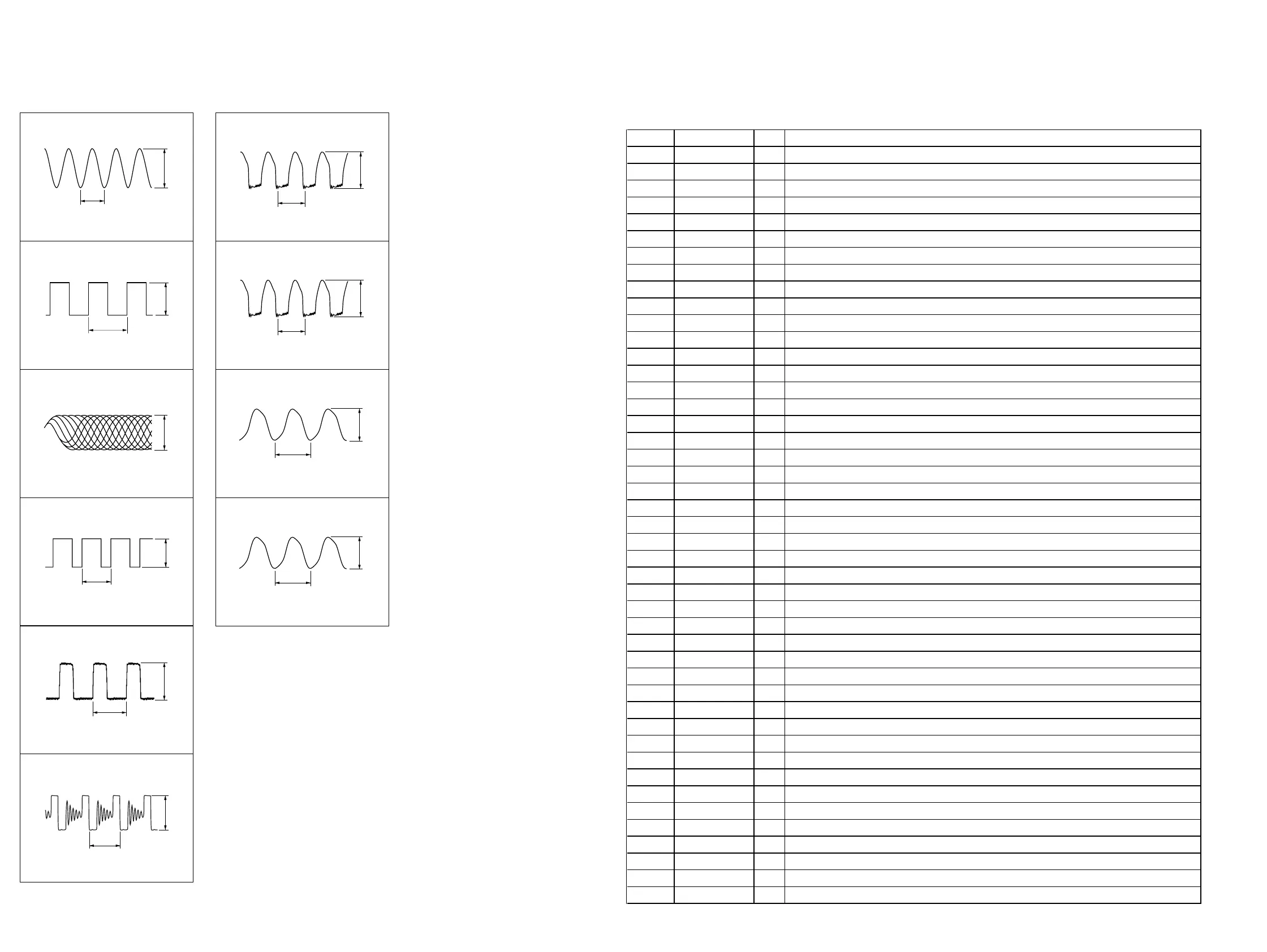
1
IC801 tg (XTAL)
500 mV/DIV, 20 ns/DIV
45.5 ns
1.1 Vp-p
8
Q104 (Collector) (FM mode)
1 V/DIV, 50 ns/DIV
195 ns
2.2 Vp-p
8
Q104 (Collector) (AM mode)
500 mV/DIV, 50 ns/DIV
195 ns
1.2 Vp-p
7
IC101 qg (X_O) (FM mode)
1 V/DIV, 5
µ
s/DIV
13.3
µ
s
1.6 Vp-p
7
IC101 qg (X_O) (AM mode)
200 mV/DIV, 5
µ
s/DIV
13.3
µ
s
0.5 Vp-p
5.7
µ
s
2.2 Vp-p
2
IC801 yd (SYNC)
(CD play mode)
1 V/DIV, 2
µ
s/DIV
4
IC401 9 (L2L)
1 V/DIV, 2
µ
s/DIV
5.7
µ
s
2.6 Vp-p
3
IC801 if (RFACI)
(CD play mode)
200 mV/DIV, 200 ns/DIV
550 mVp-p
5
IC250 5 (EXT), Q250 (Gate)
1 V/DIV, 1
µ
s/DIV
3.7
µ
s
2.2 Vp-p
6
Q250 (Drain)
2 V/DIV, 1
µ
s/DIV
3.7
µ
s
3.6 Vp-p
• IC Pin Function Description
Pin No. Pin Name I/O Description
1
FG O FG signal output to the system controller
Brake signal input terminal Not used
Comparator (W) positive pole input terminal
Comparator (V) positive pole input terminal
Comparator (U) positive pole input terminal
Comparator (U/V/W) negative pole input terminal
Dry battery connection terminal
Ground terminal
Coil connection terminal
VCC0 O Power supply voltage output terminal (+2.3V)
OSC standby signal output terminal
VCC2 O Power supply voltage output terminal (+2.1V)
VSTB2 O Power supply voltage output terminal (+2.1V)
VAPC O Power supply voltage output terminal (+1.95V)
VSTB1 O Power supply voltage output terminal (+1.25V)
VCC1 O Power supply voltage output terminal (+1.2V)
Reference voltage output terminal
VAPC power supply on/off control signal input terminal
Error amplifier output terminal for APC circuit
Delay control signal input terminal
Error amplifier output terminal for VCC0 switching power supply circuit
RF2
-
Error amplifier connection terminal for VCC0 switching power supply circuit
Error amplifier non-invert input of VCC0 switching power supply circuit
Ground terminal
O FET (bottom side) drive signal output for VD switching power supply circuit
O FET (top side) drive signal output for VD switching power supply circuit
VD I Feed back voltage input terminal for VD switching power supply circuit
Error amplifier non-invert input for VD switching power supply circuit
Error amplifier output terminal for VD switching power supply circuit
RF7
-
Error amplifier connection terminal for VD switching power supply circuit
VG power supply output terminal (+4.5V)
Capacitor connection terminal for charge pump (high side) of VG power supply circuit
Capacitor connection terminal for charge pump (low side) of VG power supply circuit
COLD ST O Not used
SYNC I 176.4 kHz clock signal input from the system controller
RMCR O Wake up signal output to the system controller
WAKE I Wake up signal input from the system controller
CLOCK I Serial clock signal input from the system controller
DATA I Serial data input from the system controller
LATCH I Latch signal input from the system controller
Focus coil drive signal (-) output terminal
Power supply terminal (for focus coil drive)
Focus coil drive signal (+) output terminal
Ground terminal (for focus/tracking coil drive)
Tracking coil drive signal (-) output terminal
MAIN BOARD IC401 TB2169AFG (O)
(FOCUS/TRACKING COIL DRIVE, SPINDLE/SLED MOTOR DRIVE, POWER CONTROL)