– 29 –
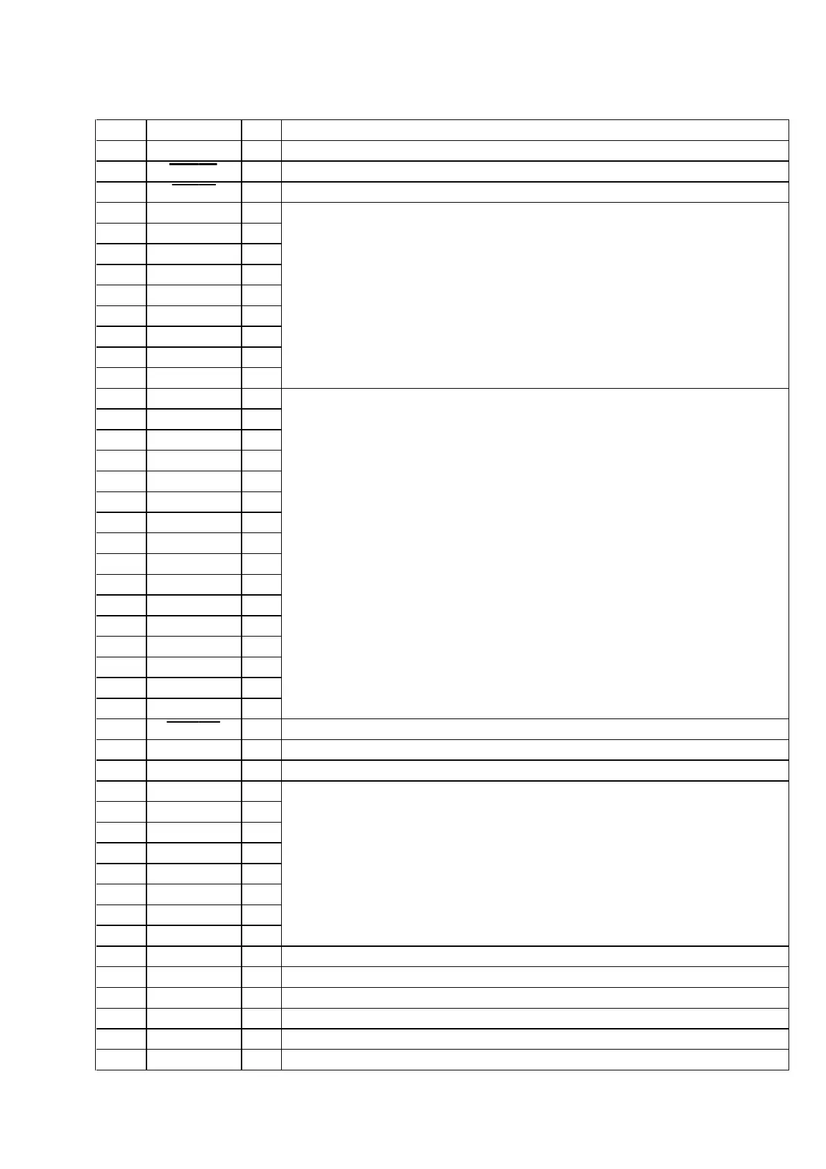
Pin No. Pin Name I/O Function
1 VCC —
Power supply terminal (+3.3V)
Row address strobe signal output to the D-RAM (IC903) “L” active
Write enable signal output to the D-RAM (IC903) “L” active
4 MA0 O
5 MA1 O
6 MA2 O
7 MA3 O
8 MA4 O
Address signal output to the D-RAM (IC903)
9 MA5 O
10 MA6 O
11 MA7 O
12 MA8 O
13
Reset signal input from the system controller (IC701) “L”: reset
Power supply terminal (+3.3V)
32 YUV0 O
33 YUV1 O
34 YUV2 O
35 YUV3 O
36 YUV4 O
37 YUV5 O
38 YUV6 O
39 YUV7 O
40 VSSCN B O
Vertical synchronous signal output to the video encoder (IC920)
Horizontal synchronous signal output to the video encoder (IC920)
System clock signal input terminal Not used (open)
System clock signal (27 MHz) input from the video encoder (IC920)
Pixel clock qualifier output for the screen video interface Not used (open)
Sub control signal output terminal Not used (open)
Two-way data bus with the D-RAM (IC903)
Video data output to the video encoder (IC920)
(YUV; Y: luminance signal, UV: Screen video interface chrominance data bus)
• MAIN BOARD (1/2) IC901 ES3210 (MPEG AUDIO/VIDEO DECODER)