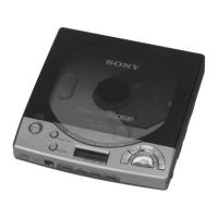
– 30 –
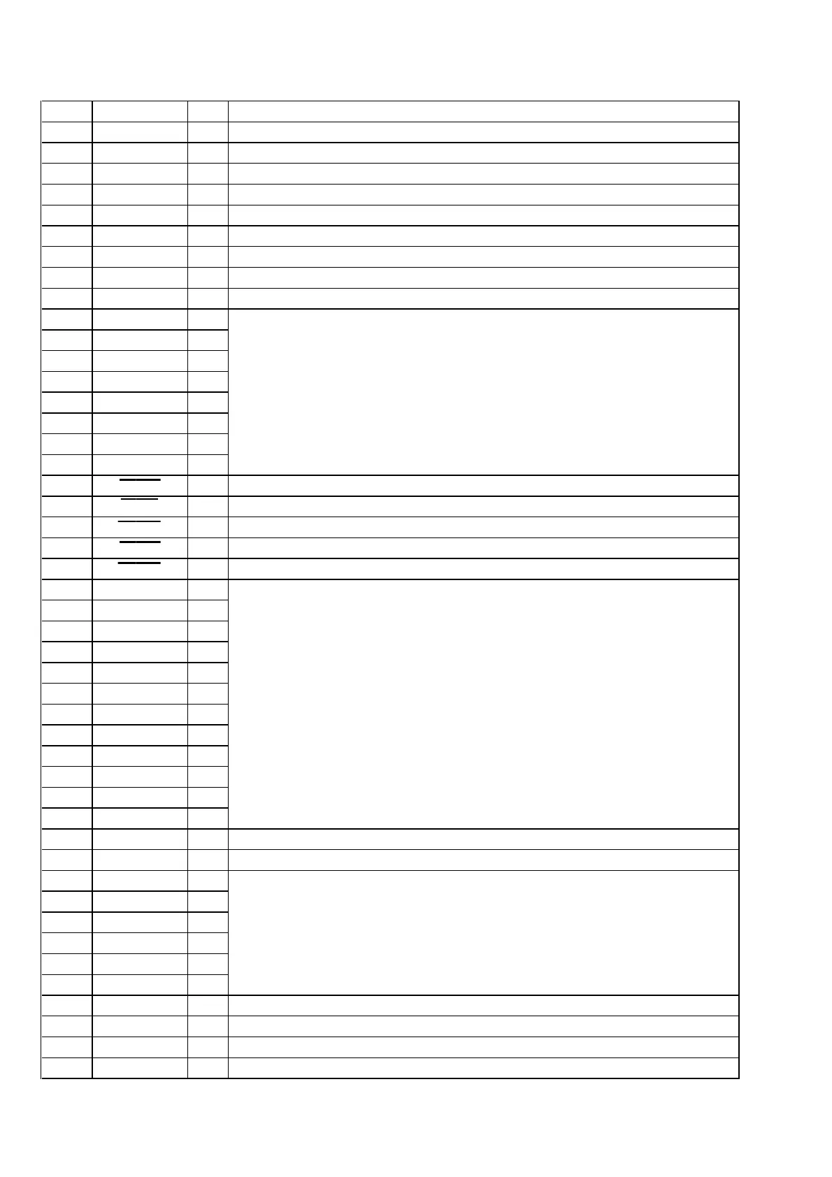
Pin No. Pin Name I/O Function
46 AUX1 I
Serial data input from the system controller (IC701)
47 AUX2 O
Serial data output to the system controller (IC701)
48 AUX3 O
NTSC/PAL mode selection signal output to the video encoder (IC920) “L”: NTSC, “H”: PAL
49 AUX4 I
C2PO signal input from the CXD2545Q (IC601)
50 VSS —
Ground terminal
51 VCC —
Power supply terminal (+3.3V)
52 AUX6 O
Communication request signal output to the system controller (IC701)
53 AUX5 I
Ready signal input from the system controller (IC701)
54 AUX7 I
Communication request signal input from the system controller (IC701)
55 LD0 I
56 LD1 I
57 LD2 I
58 LD3 I
59 LD4 I
60 LD5 I
61 LD6 I
62 LD7 I
63 LWR B O
Write enable signal output terminal “L” active Not used
64 LOE B O
Output enable signal output to the program ROM (IC902) “L” active
65 LCS3 B O
Chip select signal output to the program ROM (IC902) “L” active
66 LCS1 B I
Serial data transfer clock signal input from the system controller (IC701) “L” active
67 LCS0 B O
Chip select signal output terminal “L” active Not used (open)
68 LA0 O
69 LA1 O
70 LA2 O
71 LA3 O
72 LA4 O
73 LA5 O
74 LA6 O
75 LA7 O
76 LA8 O
77 LA9 O
78 LA10 O
79 LA11 O
80 VSS —
Ground terminal
81 VPP —
Power supply terminal (+5V) (digital system)
82 LA12 O
83 LA13 O
84 LA14 O
85 LA15 O
86 LA16 O
87 LA17 O
88 AUDIOCLK I
Audio master clock signal (16.9344 MHz) input from the D/A converter (IC320)
89 AOUT O
Audio interface serial data output to the D/A converter (IC320)
90 TBCK O
Bit clock signal (2.8224 MHz) output to the D/A converter (IC320)
91 ATFS O
L/R sampling clock signal (44.1 kHz) output to the D/A converter (IC320)
Data input from the program ROM (IC902)
Address signal output to the program ROM (IC902)
Address signal output to the program ROM (IC902)