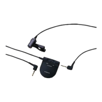
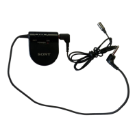
SECTION 2
DIAGRAMS
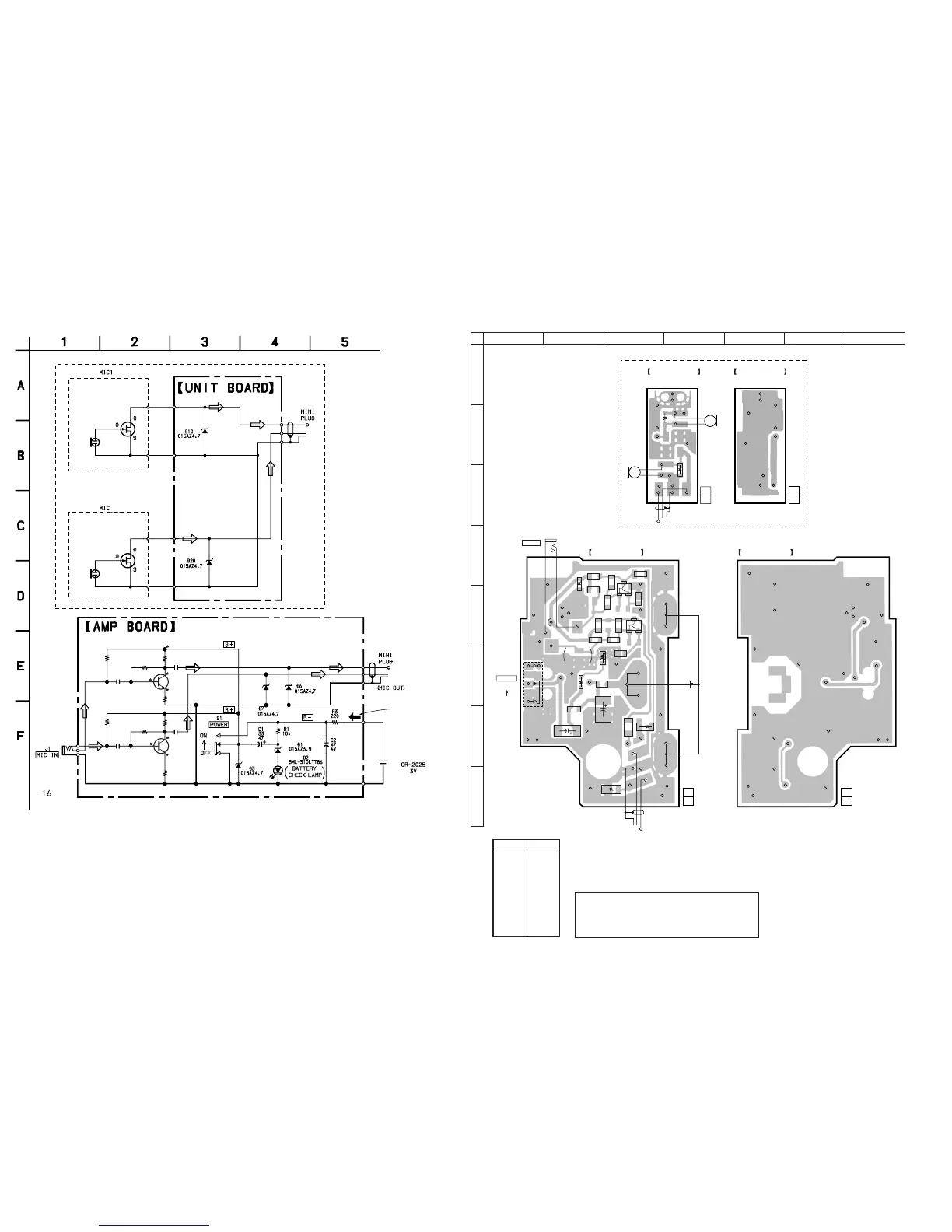
2-1. SCHEMATIC DIAGRAM
TOTAL CURRENT
MIC UNIT
CONNECT : 700uA
DISCONNECT : 460uA
LITHIUM BATTERY
(L CH)
(R CH)
2
R22
3.9K
R21
2.2M
R23
3K
C22
0.01
F
Q2
2SC4116YG
MIC AMP
R24
3K
C24
1
F
R12
2.2M
R13
3K
C12
0.01
F
C14
2.3
0.5
1.0
2.3
0.5
1.0
1
F
3.9K
R11
Q1
2SC4116YG
MIC AMP
L
R
R14
3K
2.9
MIC UNIT
2-2. PRINTED WIRING BOARD
AMP BOARD
(SIDE B)
UNIT BOARD
(SIDE B)
UNIT BOARD
(SIDE A)
AMP BOARD
(SIDE A)
1-672-000-
11
(11)
1-672-000-
11
(11)
J1
MIC IN
S1
POWER
D3
R13
R12
D1
C14
C1
C2
R1
D2
C22
R24
R22
R3
D7
R14
R11
R21
R23
C12
C24
Q2
Q1
ON
OFF
S1
(MIC OUT)
MINI
PLUG
LITHIUM
BATTERY
CR-2025
3V
BATTERY
CHECK
LAMP
16
1-673-682-
11
(11)
LR
D10
D20
MIC1
(L CH)
MINI PLUG
(MIC OUT)
MIC2
(R CH)
1-673-682-
11
(11)
D6
MIC UNIT
12
A
B
C
D
E
F
G
H
34567
Note on Schematic Diagram:
• All capacitors are in µF unless otherwise noted. pF: µµF
50 WV or less are not indicated except for electrolytics
and tantalums.
• All resistors are in Ω and
1
/
4
W or less unless otherwise
specified.
• % : indicates tolerance.
• C : panel designation.
• U : B+ Line.
• Power voltage is dc 3 V and fed with regulated dc power
supply from battery terminal.
Note on Printed Wiring Board:
• X : parts extracted from the component side.
•
®
: Through hole.
• b : Pattern of the rear side.
Caution:
Pattern face side: Parts on the pattern face side seen from
(Conductor B) the pattern face are indicated.
Parts face side: Parts on the parts face side seen from
(Component A) the parts face are indicated.
• Voltages and waveforms are dc with respect to ground
under no-signal (detuned) conditions.
• Voltages are taken with a VOM (Input impedance 10 MΩ).
Voltage variations may be noted due to normal produc-
tion tolerances.
• Signal path.
F : MIC
Ref. No. Location
D1 F-2
D2 F-3
D3 D-2
D6 H-3
D7 G-3
D10 B-3
D20 B-4
Q1 E-3
Q2 D-3
• Semiconductor
Location
— 3 — — 4 —
ECM-TS125