EasyManua.ls Logo

Sony HCD-GX9000 User Manual

Sony HCD-GX9000
78 pages
To Next Page IconTo Next Page
Page #1 background imageLoading...
Page #1 background image
HCD-GN660/GN770/
GX9000
US Model
HCD-GX9000
E Model
HCD-GN660/GN770
Australian Model
HCD-GN770
SERVICE MANUAL
MiNi Hi-Fi COMPONENT SYSTEM
Sony Corporation
Home Audio Company
Published by Sony Engineering Corporation
9-877-800-01
2004D02-1
© 2004.04
SPECIFICATIONS
Ver 1.0 2004. 04
– Continued on next page –
HCD-GN660/GN770/GX9000 are the
Amplifier, CD player, tape deck and tuner
section in MHC-GN660/GN770/GX9000.
Model Name Using Similar Mechanism HCD-GX450
CD CD Mechanism Type CDM74-F1BD81
Section Base Unit Name BU-F1BD81A
Optical Pick-up Name KSM-215DCP/C2NP
TAPE Model Name Using Similar Mechanism NEW
Section Tape Transport Mechanism Type CWM43RR35
AUDIO POWER SPECIFICATION
(MHC-GX9000 USA model only)
POWER OUTPUT AND TOTAL HARMONIC
DISTORTION:
With 6-ohm loads, both channels driven, from 120 Hz – 10 kHz;
rates 225 watts per channel minimum RMS power, with no more
than 10% total harmonic distortion from 250 miliwatts to rated
output.
Amplifier section
MHC-GX9000
Total harmonic distortion Less than 0.1%
(6 ohms at 1 kHz, 100 W)
MHC-GN770
The following are measured at
Mexican model: AC 127 V, 60 Hz
Other models: AC 120, 220, 240 V, 50/60 Hz
DIN power output (rated) 170 + 170 watts
(6 ohms at 1 kHz, DIN)
Continuous RMS power output (reference)
220 + 220 watts
(6 ohms at 1 kHz, 10% THD)
MHC-GN660
The following are measured at
Mexican model: AC 127 V, 60 Hz
Other models: AC 120, 220, 240 V, 50/60 Hz
Photo : GN770
DIN power output (rated) 150 + 150 watts
(6 ohms at 1 kHz, DIN)
Continuous RMS power output (reference)
190 + 190 watts
(6 ohms at 1 kHz, 10% THD)
Inputs
VIDEO/MD (AUDIO) IN (phono jacks):
voltage 250/450 mV, impedance 47
kiloohms
GAME (VIDEO) IN (phono jack):
1 Vp-p, 75 ohms
GAME (AUDIO) IN (phono jack):
voltage 250 mV, impedance 47 kiloohms
MIC (phone jack):
sensitivity 1 mV, impedance 10 kiloohms
Outputs
VIDEO OUT (phono jack): max. output level
1 Vp-p, unbalanced, Sync negative,
load impedance 75 ohms
PHONES (stereo mini jack):
accepts headphones of 8 ohms or more
w
w
w
.
x
i
a
o
y
u
1
6
3
.
c
o
m
Q
Q
3
7
6
3
1
5
1
5
0
9
9
2
8
9
4
2
9
8
T
E
L
1
3
9
4
2
2
9
6
5
1
3
9
9
2
8
9
4
2
9
8
0
5
1
5
1
3
6
7
3
Q
Q
TEL 13942296513 QQ 376315150 892498299
http://www.xiaoyu163.com

Table of Contents

Question and Answer IconNeed help?

Do you have a question about the Sony HCD-GX9000 and is the answer not in the manual?

Sony HCD-GX9000 Specifications

General IconGeneral
BrandSony
ModelHCD-GX9000
CategoryStereo System
LanguageEnglish

Summary

Service Manual Introduction

Service Manual Title

Title of the service manual.

Model and Specifications Overview

Key specifications for different models including power output and distortion.

General Unit Specifications

Unit Dimensions and Mass

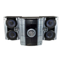
Approximate physical dimensions and weight of the unit.

Supplied Accessories

Lists accessories supplied with the unit.

Safety Check-out Procedure

Procedure for electrical safety checks like AC leakage.

Component Section Specifications

Details for disc player, tape deck, and tuner sections.

Service Manual Structure and Precautions

Servicing Notes

Important notes for service personnel, including chip component replacement.

General Information

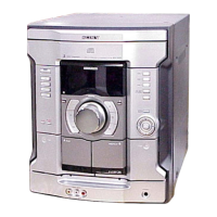
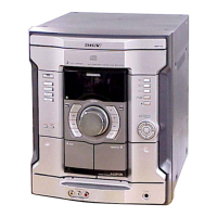
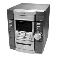
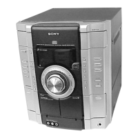
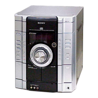
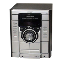
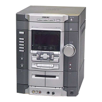
Location of controls on the main unit.

Disassembly Procedures

Step-by-step guide for disassembly of major components.

Test, Mechanical, and Electrical Adjustments

Sections covering testing and various adjustments.

Servicing Notes and Model Identification

Handling Optical Pick-up and Laser Diode

Precautions for handling the optical pick-up block and laser diode.

Laser Diode and Focus Operation Check

Procedure for checking laser diode and focus search operation.

Model Identification and Abbreviations

Information on model variants and abbreviations used.

General Controls Overview

Locating Controls on Main Unit

Identifies button locations and reference pages on the main unit.

Symbols Used for Controls

Explains symbols used for controls on the main unit.

Remote Control Operations

Remote Control Button Listing

Alphabetical list of remote control buttons and their functions.

Remote Control Symbols Explanation

Explains symbols used on the remote control.

Disassembly Procedures Overview

Disassembly Flow Chart

Outlines the overall disassembly procedure with a flow chart.

Case and Loading Panel Disassembly

Case Disassembly

Steps for removing the case.

Loading Panel Assy Disassembly

Steps for removing the loading panel assembly.

Front Panel and CD Mechanism Disassembly

Front Panel Assy Disassembly

Steps for removing the front panel assembly.

CD Mechanism Deck Disassembly

Steps for removing the CD mechanism deck.

Tape Mechanism, CD Switch Board Disassembly

Tape Mechanism and Game Board Disassembly

Steps for removing tape mechanism and game board.

CD Switch and Panel Boards Disassembly

Steps for removing CD switch and panel boards.

Switch Board and Tuner Pack Disassembly

Switch Board Disassembly

Steps for removing the switch board.

Tuner Pack Disassembly

Steps for removing the tuner pack.

Primary Board and Rear Panel Disassembly

Primary Board Disassembly

Steps for removing the primary board.

Rear Panel Disassembly

Steps for removing the rear panel.

Main Board and Surround/PA Board Disassembly

Main Board Disassembly

Steps for removing the main board.

Surround and PA Boards Disassembly

Steps for removing surround and PA boards.

Power Transformer and Driver/SW Board Disassembly

Power Transformer Disassembly

Steps for removing the power transformer.

Driver and SW Boards Disassembly

Steps for removing driver and SW boards.

BD Board, Optical Pick-Up, Sensor Board Disassembly

BD Board and Optical Pick-Up Disassembly

Steps for removing BD board and optical pick-up.

Sensor Board Disassembly

Steps for removing the sensor board.

Motor (TB) and Motor (LD) Board Disassembly

Motor (TB) Board Disassembly

Steps for removing the motor (TB) board.

Motor (LD) Board Disassembly

Steps for removing the motor (LD) board.

Test Modes Procedures

GC Test Mode Operation

Procedure to check various functions using GC test mode.

MC Test Mode Operation

Procedure to check amplifier, tuner, and tape operations.

Amplifier, Tape Function Checks

Checks for amplifier and tape functions.

Cold Reset Procedure

Procedure to perform a cold reset of the set.

Special Operational Modes

VACS ON/OFF Mode

Mode to switch VACS ON and OFF.

Tuner Step Change Mode

Procedure to change AM channel step interval.

CD Service and Aging Modes

Modes for CD sled motor control and aging check.

CD Error Code and Special Modes

CD Error Code Display Mode

How to display error codes and their meanings.

CD Repeat 5 Limit Off Mode

Mode to enable limitless CD playback repeats.

CD Ship Mode (with Memory Clear)

Mode to move optical pick-up and clear memory.

CD Operational Modes

CD Ship Mode (Without Memory Clear)

Mode to move optical pick-up for shipping.

CD Power Management Mode

Mode to switch power supply to BU during tuner function.

CD Tray Lock Mode

Mode to lock the disc trays.

Video/MD Switching Mode

Mode to switch between VIDEO and MD functions.

Mechanical and Electrical Adjustments

Mechanical Adjustments Precautions and Torque

Precautions and torque measurements for mechanical adjustments.

Electrical Adjustments: Deck Section

Electrical adjustments for the tape deck section.

Record/Playback Head Azimuth Adjustment

Procedure for adjusting record/playback head azimuth.

CD Section Adjustments and Checks

CD Section Notes and S-Curve Check Connection

Notes and connection diagram for S-curve check.

S-Curve Check Procedure and Waveforms

Steps and expected waveforms for S-curve check.

Head Adjustment Locations

Specifies adjustment locations for record/playback heads.

CD Waveform Checks

RFAC Level Check Procedure

Steps for performing RFAC level check.

E-F Balance Check Procedure

Steps for performing E-F balance check.

Waveform Diagrams and Checking Locations

Waveform diagrams and specified checking locations.

Checking Location Details

CD Board (SIDE B) Checking Location

Specifies checking location on the CD board (SIDE B).

Schematic Diagram Conventions

Schematic Diagram Notes

General notes applicable to schematic diagrams.

Printed Wiring Board Notes and Cautions

Notes and cautions for printed wiring board viewing.

Transistor Indication and Abbreviations

How transistors are indicated and explanation of abbreviations.

Circuit Board Locations Diagram

Circuit Board Layout Diagram

Diagram showing the location of various circuit boards.

Waveform Diagrams

Main Board Waveforms

Waveform examples for the main board.

BD Board Waveforms

Waveform examples for the BD board.

Panel Board Waveforms

Waveform examples for the panel board.

CD Section Block Diagram

CD Section Block Diagram

Block diagram illustrating the CD section's components and signals.

Tuner/Tape Section Block Diagram

Tuner/Tape Section Block Diagram

Block diagram illustrating the tuner and tape sections.

Main Section Block Diagram

Main Section Block Diagram

Block diagram illustrating the main section's components and signals.

Display/Power Section Block Diagram

Display/Power Section Block Diagram

Block diagram illustrating the display and power sections.

Abbreviations Used

Explanation of abbreviations used in the diagram.

BD Section Printed Wiring Board

BD Section PWB Layout

Printed wiring board layout for the BD section.

Semiconductor Locations on BD Board

Lists locations of semiconductors on the BD board.

BD Board Schematic Diagram

BD Board Schematic

Schematic diagram for the BD board.

CD Mechanism Board Printed Wiring Board

CD Mechanism PWB Layout

Printed wiring board layout for the CD mechanism board.

Semiconductor Locations on CD Mechanism Board

Lists locations of semiconductors on the CD mechanism board.

CD Mechanism Board Schematic Diagram

CD Mechanism Board Schematic

Schematic diagram for the CD mechanism board.

Main Board Printed Wiring Board

Main Board PWB Layout

Printed wiring board layout for the main board.

Semiconductor Locations on Main Board

Lists locations of semiconductors on the main board.

Main Board Schematic Diagram (Part 1)

Main Board Schematic (1/3)

Schematic diagram for the main board (part 1 of 3).

Main Board Schematic Diagram (Part 2)

Main Board Schematic (2/3)

Schematic diagram for the main board (part 2 of 3).

Main Board Schematic Diagram (Part 3)

Main Board Schematic (3/3)

Schematic diagram for the main board (part 3 of 3).

Game and CD Switch Board Printed Wiring Board

Game/CD Switch Boards PWB Layout

Printed wiring board layout for game and CD switch boards.

Semiconductor Locations on Game/CD Switch Boards

Lists locations of semiconductors on the game/CD switch boards.

Game and CD Switch Board Schematic Diagram

Game/CD Switch Boards Schematic

Schematic diagram for game and CD switch boards.

PA Board Printed Wiring Board

PA Board PWB Layout

Printed wiring board layout for the PA board.

Semiconductor Locations on PA Board

Lists locations of semiconductors on the PA board.

PA Board Schematic Diagram

PA Board Schematic

Schematic diagram for the PA board.

Panel Board Schematic Diagram (Part 1)

Panel Board Schematic (1/2)

Schematic diagram for the panel board (part 1 of 2).

Panel Board Schematic Diagram (Part 2)

Panel Board Schematic (2/2)

Schematic diagram for the panel board (part 2 of 2).

Panel Board Printed Wiring Board

Panel Board PWB Layout

Printed wiring board layout for the panel board.

Semiconductor Locations on Panel Board

Lists locations of semiconductors on the panel board.

Primary Board Printed Wiring Board

Primary Board PWB Layout

Printed wiring board layout for the primary board.

Semiconductor Locations on Primary Board

Lists locations of semiconductors on the primary board.

Primary and Surround Board Schematics

Primary Board Schematic

Schematic diagram for the primary board.

Surround Board Schematic

Schematic diagram for the surround board.

Surround Board Printed Wiring Board

Surround Board PWB Layout

Printed wiring board layout for the surround board.

Semiconductor Locations on Surround Board

Lists locations of semiconductors on the surround board.

IC Block Diagrams

Driver Board IC Block Diagrams

IC block diagrams for the driver board.

BD Board IC Block Diagrams

IC block diagrams for the BD board.

IC Pin Function Descriptions

IC101 CXD3059AR Pin Descriptions

Pin function descriptions for IC101.

IC101 CXD3059AR Pin Descriptions (Continued)

IC101 CXD3059AR Pin Descriptions

Pin function descriptions for IC101 (continued).

IC101 CXD3059AR Pin Descriptions (Continued)

IC101 CXD3059AR Pin Descriptions

Pin function descriptions for IC101 (continued).

IC901 MB90M407PF Pin Descriptions

IC901 MB90M407PF Pin Descriptions

Pin function descriptions for IC901.

IC401 M3062CMEN Pin Descriptions

IC401 M3062CMEN Pin Descriptions

Pin function descriptions for IC401.

IC401 M3062CMEN Pin Descriptions (Continued)

IC401 M3062CMEN Pin Descriptions

Pin function descriptions for IC401 (continued).

Exploded Views Introduction and Case/Rear Panel

Exploded View Notes

Notes regarding standardized parts and stocking.

Case and Rear Panel Exploded View

Exploded view of the case and rear panel section.

Front Panel Exploded View

Front Panel Exploded View

Exploded view of the front panel section.

Chassis Section Exploded View

Chassis Exploded View

Exploded view of the chassis section.

Safety-Critical Component Warning

Warning for safety-critical components.

CD Mechanism Deck Section 1 Exploded View

CD Mechanism Deck Section 1 Exploded View

Exploded view of the CD mechanism deck section 1.

CD Mechanism Deck Section 2 Exploded View

CD Mechanism Deck Section 2 Exploded View

Exploded view of the CD mechanism deck section 2.

Electrical Parts List Introduction

Electrical Parts List Notes

Notes on parts list standardization and semiconductors.

BD Board Parts List

Electrical parts list for the BD board.

Component Lists (Capacitors, Connectors, Ferrite Beads)

Lists of capacitors, connectors, and ferrite beads.

Resistors, Switches, Vibrators, Diodes Parts Lists

Resistors and Switches Parts List

Lists of resistors and switches.

Vibrator and CD SW Board Parts List

Lists of vibrator and CD SW board components.

Diodes Parts List

List of diodes with part numbers.

Driver, Game, Panel, Primary Parts Lists

Driver and Game Board Parts List

Parts list for driver and game board components.

Panel and Primary Board Parts List

Parts list for panel and primary board components.

Panel and Primary Board Parts List (Continued)

Panel and Primary Board Component Lists

Lists of capacitors, connectors, and diodes.

Main Board Parts List

Main Board Component Lists (Connectors, Diodes, Ferrite Beads, ICs)

Lists of common components for the main board.

Main Board Parts List (Continued)

Main Board Component Lists (Shorts, Transistors, Resistors)

Lists of short chips, transistors, and resistors.

Main Board Parts List (Continued)

Main Board Resistor List

List of resistors with part numbers and values.

Main Board Parts List (Continued)

Main Board Resistor List

List of resistors with part numbers and values.

Motor, PA Board Parts List

PA Board Parts List (Continued)

PA Board Component Lists (ICs, Shorts, Transistors, Resistors)

Lists of various components for the PA board.

Panel and Primary Board Parts List (Continued)

Panel and Primary Board Component Lists (Capacitors, Connectors, Diodes)

Lists of various components for panel and primary boards.

Panel Board Parts List (Continued)

Panel and Primary Board Parts List (Continued)

Primary, Sensor, Surround Board Parts List

Primary, Sensor, Switch Board Parts List

Parts list for primary, sensor, and switch boards.

Motor, PA Board Parts List (Continued)

Motor and PA Board Component Lists (Transformers)

Lists of transformers for motor and PA boards.

Safety-Critical Component Warning

Warning for safety-critical components.

Related product manuals