EasyManua.ls Logo

Sony HCD-GX255 User Manual

Sony HCD-GX255
138 pages
To Next Page IconTo Next Page
Page #1 background imageLoading...
Page #1 background image
SERVICE MANUAL
COMPACT DISC DECK RECEIVER
HCD-GX255/RG170/RG470
Ver. 1.2 2005.09
9-879-612-03
2005I05-1
© 2005.09
Sony Corporation
Personal Audio Group
Published by Sony Engineering Corporation
– Continued on next page –
Canadian Model
HCD-GX255
AEP Model
E Model
HCD-RG170/RG470
Australian Model
HCD-RG170
Photo: HCD-GX255
HCD-GX255 is the amplifier, CD player, tape
deck and tuner section in MHC-GX255.
HCD-RG170 is the amplifier, CD player, tape
deck and tuner section in MHC-RG170.
HCD-RG470 is the amplifier, CD player, tape
deck and tuner section in MHC-RG470.
SPECIFICATIONS
Model Name Using Similar Mechanism NEW
CDM74KFS-F1BD81C (Except Mexican model) or
CD Mechanism Type CDM74KFS-K6BD83S (Canadian, AEP, East European, Russian, E2, E51 models)/
CD CDM74KFS-F1BD84 (Mexican model)
Section BU-F1BD81C (Except Mexican model) or
Base Unit Name BU-K6BD83S-WOD (Canadian, AEP, East European, Russian, E2, E51 models)/
BU-F1BD84 (Mexican model)
Optical Pick-up Block Name KSM-215DCP or KSM-213DCP
TAPE Model Name Using Similar Mechanism HCD-GX355/RG270
Section Tape Transport Mechanism Type CWM43FF13
Amplifier section
Canadian model:
HCD-GX255
Continuous RMS power output (reference):
65 + 65 watts (6 ohms at
1kHz, 10% THD)
Total harmonic distortion less than 0.07% (6 ohms at
1kHz, 40 W)
European and Russian models:
HCD-RG470
DIN power output (rated): 110 + 110 watts (6 ohms at
1kHz, DIN)
Continuous RMS power output (reference):
140 + 140 watts (6 ohms at
1kHz, 10% THD)
Music power output (reference):
280 + 280 watts (6 ohms at
1kHz, 10% THD)
HCD-RG170
DIN power output (rated): 20 + 20 watts (6 ohms at
1kHz, DIN)
Continuous RMS power output (reference):
25 + 25 watts (6 ohms at
1kHz, 10% THD)
Music power output (reference):
50 + 50 watts (6 ohms at
1kHz, 10% THD)
Other models:
HCD-RG470
The following measured at AC 120, 127, 220, 240 V
50/60 Hz
DIN power output (rated): 130 + 130 watts (6 ohms at
1kHz, DIN)
Continuous RMS power output (reference):
160 + 160 watts (6 ohms at
1kHz, 10% THD)
HCD-RG170
The following measured at AC 120, 127, 220, 240 V
50/60 Hz
DIN power output (rated): 50 + 50 watts (6 ohms at
1kHz, DIN)
Continuous RMS power output (reference):
65 + 65 watts (6 ohms at
1kHz, 10% THD)
Inputs
AUDIO IN (stereo mini jack):
voltage 250 mV,
impedance 47 kilohms
MIC (phone jack) (Latin American model only):
sensitivity 1 mV,
impedance 10 kilohms
Outputs
PHONES (stereo mini jack):
accepts headphones of
8ohms or more
VIDEO OUT (phono jack) (Mexican model only):
max. output level 1Vp-p,
unbalanced, Sync
negative, load impedance
75 ohms
SPEAKER: accepts impedance of 6 to
16 ohms
Abbreviation
E2 : 120V AC area in E model
E51 : Chilean and Peruvian models

Table of Contents

Question and Answer IconNeed help?

Do you have a question about the Sony HCD-GX255 and is the answer not in the manual?

Sony HCD-GX255 Specifications

General IconGeneral
TypeMini Hi-Fi Component System
CD PlayerYes
Number of Discs1
TunerFM/AM
Preset Stations30 (20 FM, 10 AM)
Speakers2-way speakers
Remote ControlYes
USB PortNo
FunctionsRadio
Playable File TypesMP3
WeightMain Unit: 4.2 kg

Summary

SPECIFICATIONS

Amplifier section

Details amplifier specifications for different models and regions.

Inputs

Lists the available input types and their electrical characteristics.

Outputs

Lists the available output types and their electrical characteristics.

CD player section

Laser Diode Properties

Details laser diode properties including emission duration and output power.

Tape deck section

Frequency response

Specifies the frequency response range for tape playback.

Tuner section

FM tuner section

Details tuning ranges and intermediate frequencies for FM reception.

AM tuner section

Details tuning ranges and intermediate frequencies for AM reception.

General

Power requirements

Lists the required power input voltages and frequencies for various regions.

Power consumption

Details power consumption in watts for different models and standby mode.

Dimensions (w/h/d) (excl. speakers)

Provides the physical dimensions of the unit excluding speakers.

Mass (excl. speakers)

Lists the weight of the unit excluding speakers for different models.

UNLEADED SOLDER

SERVICING NOTES

NOTES ON HANDLING THE OPTICAL PICK-UP BLOCK OR BASE UNIT

Precautions for handling the optical pick-up block and flexible boards due to electrostatic sensitivity.

NOTES ON LASER DIODE EMISSION CHECK

Instructions for safely checking laser diode emission, emphasizing distance from the objective lens.

LASER DIODE AND FOCUS SEARCH OPERATION CHECK

Steps to check laser diode and focus search operation using the 'S curve check'.

DISCRIMINATION OF THE MAIN BOARD

How to differentiate between Suffix-11 and Suffix-12 main boards used in sets.

GENERAL

Location of Controls

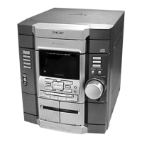
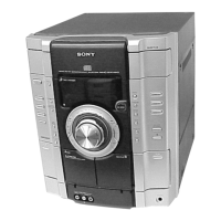
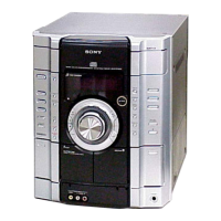
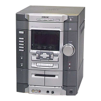
Diagrams and labels for all controls and buttons on the main unit.

DISASSEMBLY

3-1. DISASSEMBLY FLOW

A flowchart illustrating the order of disassembly for the set's components.

3-2. CASE (TOP)

Procedure and illustration for removing the top case of the unit.

3-3. DOOR (CD)

Procedure for disassembling the CD door, including turning a pulley.

3-4. FRONT PANEL SECTION

Steps for removing the front panel assembly, showing connectors and screws.

3-5. MECHANICAL DECK (CWM43FF13)

Instructions for disassembling the mechanical CD deck mechanism (CWM43FF13).

3-6. CD MECHANISM DECK (CDM74KFS-F1BD81C (EXCEPT MX MODEL)/CDM74KFS-F1BD84 (MX MODEL))

Procedure for removing the CD mechanism deck, detailing screws and wire connections.

3-7. BACK PANEL SECTION

Steps to remove the back panel section, showing connectors and screws.

3-8. MAIN Board

Procedure for removing the main board, showing connectors and screws.

3-9. BD BOARD/CD BOARD

Instructions for removing the BD board or CD board, noting soldering points.

3-10. DRIVER BOARD, SW BOARD

Steps to remove the driver board and SW board, showing connectors and screws.

3-11. OPTICAL PICK-UP BLOCK (KSM-215DCP)

Procedure for removing the optical pick-up block, including insulators and springs.

3-12. SENSOR BOARD

Instructions for removing the sensor board, showing screws and connectors.

3-13. MOTOR (TB) BOARD

Steps to remove the motor (TB) board, detailing motor soldering points.

3-14. MOTOR (LD) BOARD

Procedure for removing the motor (LD) board, including motor soldering points.

TEST MODE

MC COLD RESET

Procedure to clear all preset data and return the set to initial conditions.

AM TUNING INTERVAL CHANGE-OVER

How to change the AM tuning interval between 9 kHz and 10 kHz.

CD SHIP (LOCK) MODE

Moves the optical pick-up to a vibration-resistant position for customer return.

CD SHIP (LOCK) MODE & COLD RESET

Simultaneously performs CD ship (lock) mode and cold reset.

CD TRAY LOCK MODE

Disables disc tray operation for shop display, preventing sample disc removal.

AMP TEST MODE

Displays amplifier IC parameters and VACS status, including equalizer adjustment.

AGING MODE

Display at the Aging Mode

Displays operating states of CD and tape deck sections alternately.

CD Section

Details the aging sequence for the CD section operations.

Tape Deck Section

Details the aging sequence for the tape deck section operations.

PANEL TEST MODE

MC TEST MODE

Mechanism Deck Error Code Mode

Displays mechanism deck error codes in a 10-character format.

VERSION DISPLAY MODE

CD ERROR CODE DISPLAY MODE

The 5th and 6th digit from the left indicates: (Error step display)

The 7th and 8th digit from the left indicates: (Motor status display)

The 9th and 10th digit from the left indicates: (Tray status display)

2. Optical Pick-up Error Code Mode

5 REPEAT LIMIT CANCEL MODE

ELECTRICAL ADJUSTMENTS

CD SECTION

Notes and procedures for CD section checks and adjustments.

S-CURVE CHECK

Procedure to check the S-curve waveform symmetry and peak-to-peak level.

RFAC LEVEL CHECK

Procedure to check the RFAC signal waveform clarity and level.

DIAGRAMS

6-1. BLOCK DIAGRAM – CD SERVO Section –

Block diagram illustrating the CD servo system signal flow and components.

6-2. BLOCK DIAGRAM – AUDIO/VIDEO Section –

Block diagram showing the audio and video signal paths and associated circuitry.

6-3. BLOCK DIAGRAM – AMP Section –

Block diagram detailing the amplifier section, including power, protection, and speaker outputs.

6-4. BLOCK DIAGRAM – PANEL, POWER SUPPLY Section –

Block diagram of the panel controls, power supply, and voltage regulation circuits.

6-5. PRINTED WIRING BOARD – CD Board – (Except MX model)

Printed wiring board layout for the CD board (excluding Mexican models), showing component placement.

6-6. SCHEMATIC DIAGRAM – CD Board – (Except MX model)

Schematic diagram for the CD board (excluding Mexican models), detailing circuit connections.

6-7. PRINTED WIRING BOARD – BD Board – (MX model only)

Printed wiring board layout for the BD board (Mexican models only), showing component placement.

6-8. SCHEMATIC DIAGRAM – BD Board – (MX model only)

Schematic diagram for the BD board (Mexican models only), detailing circuit connections.

6-9. PRINTED WIRING BOARDS – CHANGER Section –

Printed wiring board layouts for the changer section components.

6-10. SCHEMATIC DIAGRAM – CHANGER Section –

Schematic diagram for the changer section, illustrating its circuitry.

6-11. PRINTED WIRING BOARD – MAIN Board – (Suffix-11)

Printed wiring board layout for the main board (Suffix-11), showing component placement.

6-12. SCHEMATIC DIAGRAM – MAIN Board (1/3) – (Suffix-11)

Schematic diagram for the main board, part 1 of 3 (Suffix-11).

6-13. SCHEMATIC DIAGRAM – MAIN Board (2/3) – (Suffix-11)

Schematic diagram for the main board, part 2 of 3 (Suffix-11).

6-14. SCHEMATIC DIAGRAM – MAIN Board (3/3) – (Suffix-11)

Schematic diagram for the main board, part 3 of 3 (Suffix-11).

6-15. PRINTED WIRING BOARD – MAIN Board – (Suffix-12)

Printed wiring board layout for the main board (Suffix-12), showing component placement.

6-16. SCHEMATIC DIAGRAM – MAIN Board (1/3) – (Suffix-12)

Schematic diagram for the main board, part 1 of 3 (Suffix-12).

6-17. SCHEMATIC DIAGRAM – MAIN Board (2/3) – (Suffix-12)

Schematic diagram for the main board, part 2 of 3 (Suffix-12).

6-18. SCHEMATIC DIAGRAM – MAIN Board (3/3) – (Suffix-12)

Schematic diagram for the main board, part 3 of 3 (Suffix-12).

6-19. PRINTED WIRING BOARD – POWER Board – (GX255/RG170)

Printed wiring board layout for the power board (GX255/RG170), showing component placement.

6-20. SCHEMATIC DIAGRAM – POWER Board – (GX255/RG170)

Schematic diagram for the power board (GX255/RG170), detailing circuit connections.

6-21. PRINTED WIRING BOARD – POWER Board – (RG470: AEP, EE, RU)

Printed wiring board layout for the power board (RG470 models AEP, EE, RU).

6-22. SCHEMATIC DIAGRAM – POWER Board – (RG470: AEP, EE, RU)

Schematic diagram for the power board (RG470 models AEP, EE, RU).

6-23. PRINTED WIRING BOARD – POWER Board – (RG470: E2, E51, AR, MX)

Printed wiring board layout for the power board (RG470 models E2, E51, AR, MX).

6-24. SCHEMATIC DIAGRAM – POWER Board – (RG470: E2, E51, AR, MX)

Schematic diagram for the power board (RG470 models E2, E51, AR, MX).

6-25. PRINTED WIRING BOARDS – AUDIO IN, MIC, HEADPHONE Boards –

Printed wiring board layouts for the audio input, microphone, and headphone boards.

6-26. SCHEMATIC DIAGRAM – AUDIO IN, MIC, HEADPHONE Boards –

Schematic diagram for the audio input, microphone, and headphone sections.

6-27. PRINTED WIRING BOARDS – CD-G Section – (MX model only)

Printed wiring board layout for the CD-G section (Mexican models only).

6-28. SCHEMATIC DIAGRAM – CD-G Section – (MX model only)

Schematic diagram for the CD-G section (Mexican models only).

6-29. PRINTED WIRING BOARD – PANEL Section (1/2) –

Printed wiring board layout for the panel section, part 1 of 2.

6-30. PRINTED WIRING BOARD – PANEL Section (2/2) –

Printed wiring board layout for the panel section, part 2 of 2.

6-31. SCHEMATIC DIAGRAM – PANEL Section (1/2) –

Schematic diagram for the panel section, part 1 of 2.

6-32. SCHEMATIC DIAGRAM – PANEL Section (2/2) –

Schematic diagram for the panel section, part 2 of 2.

6-33. PRINTED WIRING BOARDS – TRANS Section – (GX255/RG170) –

Printed wiring board layouts for the transformer section (GX255/RG170).

6-34. SCHEMATIC DIAGRAM – TRANS Section – (GX255/RG170) –

Schematic diagram for the transformer section (GX255/RG170).

6-35. PRINTED WIRING BOARDS – TRANS Section – (RG470: AEP, EE, RU) –

Printed wiring board layouts for the transformer section (RG470 models AEP, EE, RU).

6-36. SCHEMATIC DIAGRAM – TRANS Section – (RG470: AEP, EE, RU) –

Schematic diagram for the transformer section (RG470 models AEP, EE, RU).

6-37. PRINTED WIRING BOARDS – TRANS Section – (RG470: E2, E51, AR, MX) –

Printed wiring board layouts for the transformer section (RG470 models E2, E51, AR, MX).

6-38. SCHEMATIC DIAGRAM – TRANS Section – (RG470: E2, E51, AR, MX) –

Schematic diagram for the transformer section (RG470 models E2, E51, AR, MX).

• Waveforms

Illustrations of key waveforms from various boards for analysis.

IC Block Diagrams

Block diagrams detailing the internal structure of key integrated circuits.

IC Pin Function Description

MAIN BOARD IC901 M30302MCP-A02FPU0 (SYSTEM CONTROLLER)

Pinout and function description for the System Controller IC on the main board.

EXPLODED VIEWS

7-1. OVERALL SECTION

Overall exploded view of the set, showing major assemblies and part numbers.

7-2. BACK PANEL SECTION

Exploded view of the back panel assembly, detailing parts and wires.

7-3. FRONT PANEL SECTION

Exploded view of the front panel section, listing controls, keys, and boards.

7-4. KEY SECTION

Exploded view focusing on the key mechanisms and related parts.

7-5. CHASSIS SECTION

Exploded view of the chassis assembly, showing main boards and power components.

7-6. TRANSFORMER SECTION

Exploded view of the transformer section, including power transformers and fuses.

7-7. CD MECHANISM DECK SECTION-1 (CDM74KFS-K6BD83S)

Exploded view of the CD mechanism deck, part 1, detailing internal components.

7-8. CD MECHANISM DECK SECTION-2 (CDM74KFS-K6BD83S)

Exploded view of the CD mechanism deck, part 2, showing the mechanical assembly.

ELECTRICAL PARTS LIST

SUPPLEMENT-1

1. NEW/FORMER TYPE DISCRIMINATION

Procedure to distinguish between new and former types of the unit using test mode.

ELECTRICAL ADJUSTMENT

CD SECTION

Notes and procedures for CD section checks and adjustments.

FOCUS BIAS CHECK

Procedure to check the focus bias when the optical pick-up block is replaced.

3-1. PRINTED WIRING BOARD – CD Board (Component Side) –

3-2. SCHEMATIC DIAGRAM – CD Board –

3-3. PRINTED WIRING BOARD – MAIN Board –

3-4. SCHEMATIC DIAGRAM – MAIN Board (1/3) –

3-5. SCHEMATIC DIAGRAM – MAIN Board (2/3) –

3-6. SCHEMATIC DIAGRAM – MAIN Board (3/3) –

3-7. PRINTED WIRING BOARD – HEADPHONE Board –

3-8. SCHEMATIC DIAGRAM – HEADPHONE Board –

IC Block Diagram

– CD Board –

Block diagram for the CD board's IC.

– MAIN Board – IC101 BD3401KS2

IC Pin Function Description

CD BOARD IC201 CXD3014A-201R (CD DSP)

Pinout and function description for the CD DSP IC on the CD board.

EXPLODED VIEWS

4-1. FRONT PANEL SECTION

Exploded view of the front panel section, listing controls, keys, and boards.

4-2. CHASSIS SECTION

Exploded view of the chassis assembly, showing main boards and power components.

4-3. CD MECHANISM DECK SECTION-1 (CDM74KFS-K6BD83S)

Exploded view of the CD mechanism deck, part 1, detailing internal components.

4-4. CD MECHANISM DECK SECTION-2 (CDM74KFS-K6BD83S)

Exploded view of the CD mechanism deck, part 2, showing the mechanical assembly.

ELECTRICAL PARTS LIST

MEMO

REVISION HISTORY

Related product manuals