4-77
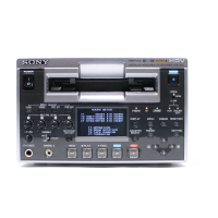
HVR-M10C/M10E/M10J/M10N/M10P/M10U
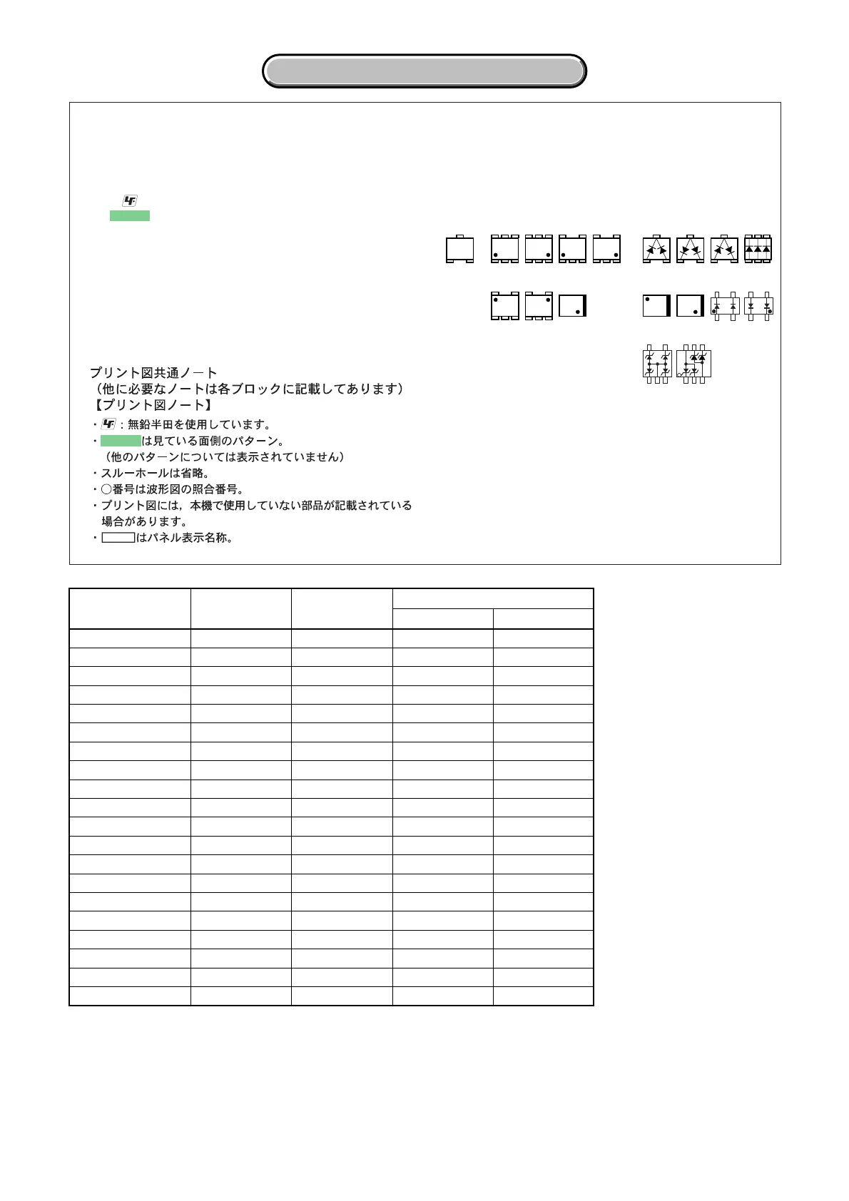
4-3. PRINTED WIRING BOARDS
4-3. PRINTED WIRING BOARDS
board name
FP-230
FP-971
FP-976
FP-977
HP-139
JL-001
FP-090
JU-001
FP-095
LI-073
MR-048
PD-222
PW-129
SW-436
VA-120
FP-088
FP-089
DA-033
DB-018
VC-367
parts location
(shown on page)
–
–
–
–
–
4-128
–
4-128
–
–
–
4-128
–
4-128
4-129
–
–
4-129
4-130
4-131 to 133
number of layers
2
2
2
2
2
2
1
2
1
2
4
2
2
2
4
1
1
6
6
8
layers not shown
–
–
–
–
–
–
–
–
–
–
2 to 3
–
–
–
2 to 3
–
–
2 to 5
2 to 5
2 to 7
pattern
BOARD INFORMATION
waveforms
(shown on page)
–
–
–
–
–
–
–
–
–
–
4-125
4-126
–
–
4-126
–
–
–
–
4-127
(For printed wiring boards)
•
: Uses unleaded solder.
•
: Pattern from the side which enables seeing.
(The other layers’ patterns are not indicated)
• Through hole is omitted.
• Circled numbers refer to waveforms.
• There are a few cases that the part printed on diagram
isn’t mounted in this model.
• C: panel designation
(ENGLISH)
THIS NOTE IS COMMON FOR WIRING BOARDS
(In addition to this, the necessary note is printed in each block)
21
3
21
3
21
3
345
21
123
654
EB
C
31
5
5
2
46
123
54
43
12
5
4
1
3
12
43
312
45
534
12
34
21
12
43
46
2
5
31
12
4
3
64
1
3
• Chip parts
Transistor Diode
(JAPANESE)