4-13
4-14
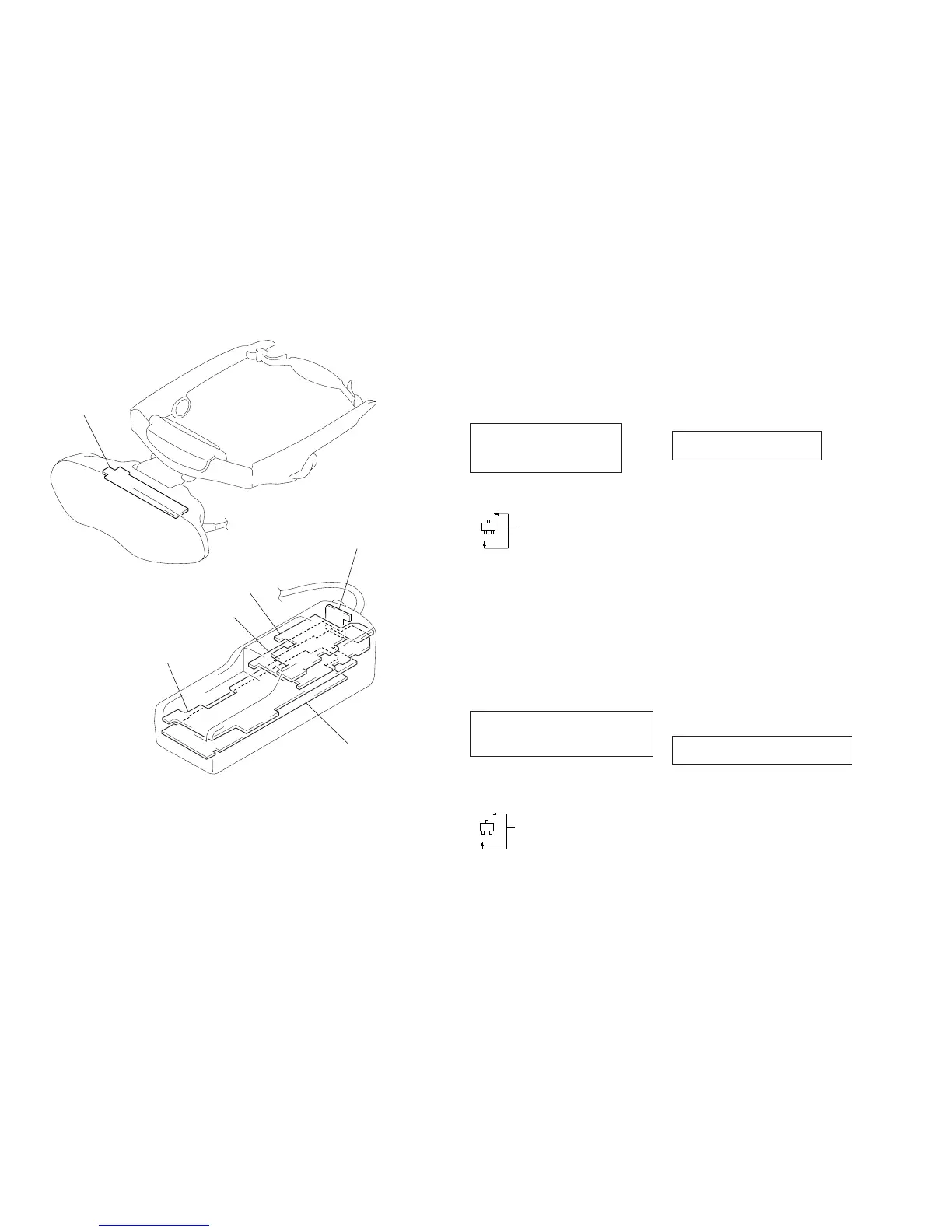
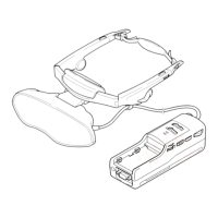
• Circuit Boards Location
4-6. プリント図,回路図共通ノート
(他に必要なノートは各セクションに記載してあります)
NOTE FOR PRINTED WIRING BOARDS AND SCHEMATIC DIAGRAMS
(In addition to this, the necessary note is printed ineach block)
Note on Schematic Diagram:
• All capacitors are in µF unless otherwise noted. pF: µµF
50 WV or less are not indicated except for electrolytics
and tantalums.
• All resistors are in Ω and
1
/
4
W or less unless otherwise
specified.
•
f
: internal component.
• C : panel designation.
Note on Printed Wiring Board:
• X : parts extracted from the component side.
• Y : parts extracted from the conductor side.
• b : Pattern from the side which enables seeing.
(The other layers' patterns are not indicated.)
• U : B+ Line.
• Power voltage is dc 8.4 V and fed with regulated dc power
supply from external power voltage jack.
• Voltages and waveforms are dc with respect to ground in
color-bar signal input.
no mark : VIDEO MODE
• Voltages are taken with a VOM (Input impedance 10 MΩ).
Voltage variations may be noted due to normal produc-
tion tolerances.
• Waveforms are taken with a oscilloscope.
Voltage variations may be noted due to normal produc-
tion tolerances.
• Circled numbers refer to waveforms.
• Signal path.
F : AUDIO
L : VIDEO
Note: The components identified by mark 0 or dotted line
with mark 0 are critical for safety.
Replace only with part number specified.
Caution:
Pattern face side: Parts on the pattern face side seen from
(Side B) the pattern face are indicated.
Parts face side: Parts on the parts face side seen from
(Side A) the parts face are indicated.
• JK-136 (F), YC-148 (F), MA-324 (F), LC-61 (F), SW-306
(F), and DD-107 (F) boards are multi-layer printed board.
However, the patterns of intermediate-layer have not been
included in the diagram.
• Indication of transistor
LC-61 (F) board
JK-136 (F) board
SW-306 (F) board
DD-107 (F) board
YC-148 (F) board
MA-324 (F) boar
プリント図ノート
・ X :部品面側取付のリード線。
・ Y :パターン面側取付のリード線。
・ b :見ている面側のパターン。
(他のパターンについては,表示されていません。)
注意
パターン面側: パターン面より見たパターン面側
(SIDEB) の部品が記載されています。
部品面側: 部品面より見た部品面側の部品が
(SIDEA) 記載されています。
回路図ノート
・ケミコン,タンタルを除くコンデンサで,耐圧50V以下のもの
は,その耐圧を省略。単位はすべて µF(p は pF)。
・抵抗で指示のないものは 1/4W 以下を示す。単位はすべてΩ。
・
f
印は内蔵部品。
・ C :パネル表示名称。
・ U :B +ライン。
・電源は外部電源ジャックより安定化電源で DC8.4V を供給。
・電圧および波形は,対アース間をカラーバー信号入力状態で
測定。
無 印:VIDEO モード
・電圧値は,テスタ(入力インピーダンス 10M Ω)で測定した
参考値。
・波形図は,オシロスコープで測定した参考図。
・
a
番号は波形図の照合番号。
・信号の流れについて
F :AUDIO
L :VIDEO
0 印の部品,または 0 印付きの点線で囲まれた部品
は,安全性を維持するために重要な部品です。
従って交換時は,必ず指定の部品を使用して下さい。
・JK-136(F),YC-148(F),MA-324(F),LC-61(F),SW-
306(F),DD-107(F)基板は多層構造のプリント基板ですが,
中間層のパターン図は掲載していません。
・トランジスタ表示
C
B
These are omitted.
E
Q