– 3 –
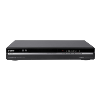
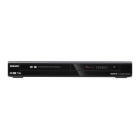
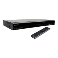
RDR-GX257/GX380
TABLE OF CONTENTS
Section Title Page Section Title Page
1. SERVICE NOTE
1-1. EEPROM IC Setting ..................................................... 1-1
1-2. Disc Removal Procedure If The Tray Cannot Be
Ejected (Forced Ejection) ............................................. 1-2
1-3. How To Distinguish Difference Of AEP Model .............. 1-2
2. DISASSEMBLY
2-1. Disassembly Flow ........................................................ 2-1
2-2. Top Case ...................................................................... 2-1
2-3. Front Panel ................................................................... 2-2
2-4. Mechanism Deck .......................................................... 2-2
2-5. IO Board ....................................................................... 2-3
2-6. Circuit Boards Location ................................................ 2-3
3. BLOCK DIAGRAMS
3-1. Overall Block Diagram
(US, Canadian, E, Australian, Singapore) .................... 3-1
3-2. Overall Block Diagram (AEP, UK, Russian) ................. 3-2
3-3. Power Block Diagram ................................................... 3-3
4. SCHEMATIC DIAGRAMS
4-1. Frame Schematic Diagram (1/2) .................................. 4-1
4-2. Frame Schematic Diagram (2/2) .................................. 4-2
4-3. IO Board (SMPS) Schematic Diagram (1/4)................. 4-3
4-4. IO Board (MICOM/TUNER)
Schematic Diagram (2/4).............................................. 4-4
4-5. IO Board (CONNECTOR/AV SWITCH/JACK)
Schematic Diagram (3/4).............................................. 4-5
4-6. IO Board (V DECODER/A.DAC/MIC INPUT)
Schematic Diagram (4/4).............................................. 4-6
4-7. MAIN Board (MPEG) Schematic Diagram (1/5) ........... 4-7
4-8. MAIN Board (DDR/LATCH/FLASH/RESET)
Schematic Diagram (2/5).............................................. 4-8
4-9. MAIN Board (DV1394/INTERFACE CONNECTOR)
Schematic Diagram (3/5).............................................. 4-9
4-10. MAIN Board (RF/MOTOR DRIVE)
Schematic Diagram (4/5).............................................. 4-10
4-11. MAIN Board (DSP) Schematic Diagram (5/5) .............. 4-11
4-12. HDMI Board (HDMI CONNECTOR)
Schematic Diagram ...................................................... 4-12
4-13. TIMER Board (FL DRIVER)
Schematic Diagram (1/2).............................................. 4-13
4-14. TIMER Board (AV INPUT/USB INPUT/DV1394 INPUT)
Schematic Diagram (2/2).............................................. 4-14
4-15. KEY Board (POWER SWITCH) Schematic Diagram ... 4-15
4-16. Waveforms ................................................................... 4-16
4-17. Circuit Voltage Chart .................................................... 4-24
5. PRINTED WIRING BOARDS
5-1. IO Board (IO/SMPS) Printed Wiring Board
(Component Side) ........................................................ 5-1
5-2. IO Board (IO/SMPS) Printed Wiring Board
(Conductor Side) .......................................................... 5-2
5-3. MAIN Board (MAIN/LOADER) Printed Wiring Board
(Component Side) ........................................................ 5-3
5-4. MAIN Board (MAIN/LOADER) Printed Wiring Board
(Conductor Side) .......................................................... 5-4
5-5. HDMI Board (HDMI CONNECTOR)
Printed Wiring Board .................................................... 5-5
5-6. TIMER Board (FRONT) Printed Wiring Board.............. 5-6
5-7. KEY Board (POWER SWITCH)
Printed Wiring Board .................................................... 5-7
6. TROUBLESHOOTING ............................................. 6-1
7. REPAIR PARTS LIST
7-1. Exploded Views ............................................................ 7-1
7-1-1. Case Section ........................................................... 7-1
7-1-2. Mechanism Deck Section ........................................ 7-2
7-1-3. Accessories ............................................................. 7-3
7-2. Electrical Parts List ....................................................... 7-4
w
w
w
.
x
i
a
o
y
u
1
6
3
.
c
o
m
Q
Q
3
7
6
3
1
5
1
5
0
9
9
2
8
9
4
2
9
8
T
E
L
1
3
9
4
2
2
9
6
5
1
3
9
9
2
8
9
4
2
9
8
0
5
1
5
1
3
6
7
3
Q
Q
TEL 13942296513 QQ 376315150 892498299
TEL 13942296513 QQ 376315150 892498299
http://www.xiaoyu163.com
http://www.xiaoyu163.com
 Loading...