1111
RM-AV3000
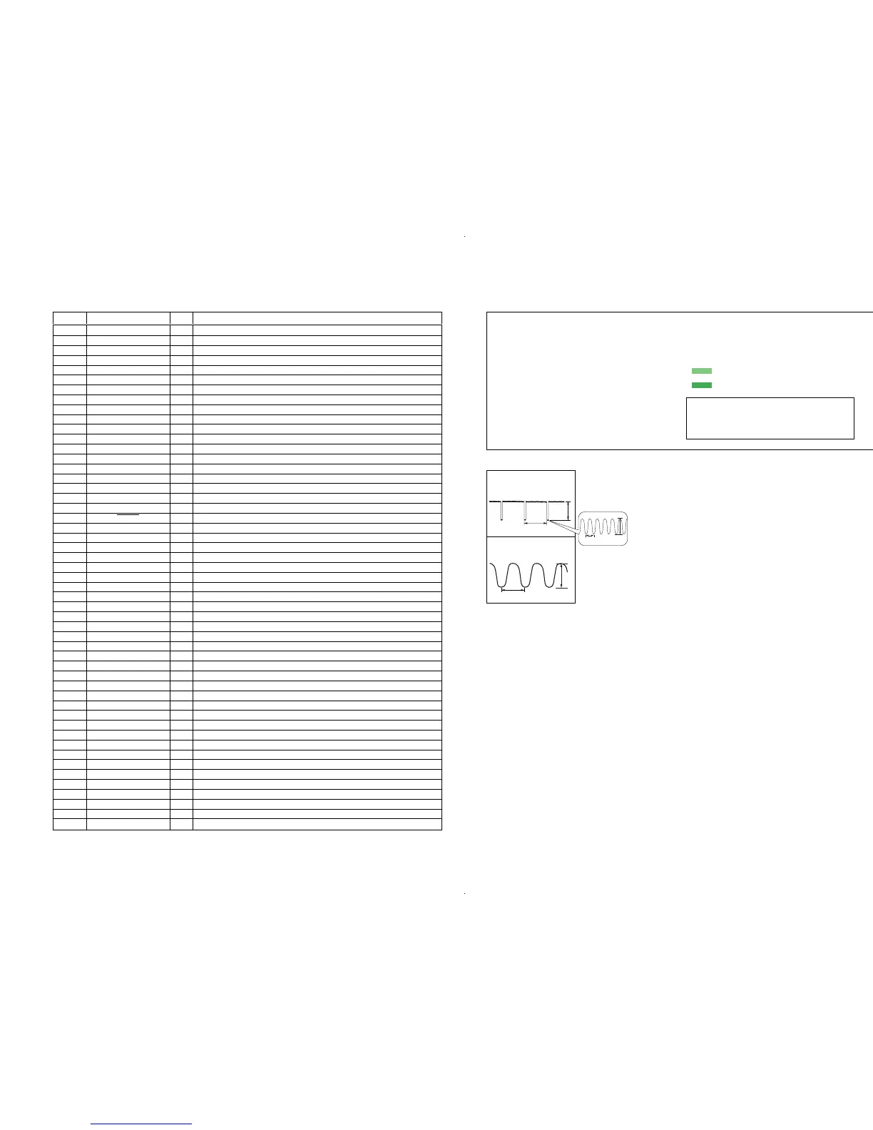
4-1. IC Pin Function
• IC1 (µPD703033AGF-A27-3BA) (SYSTEM CONTROL)
SECTION 4
DIAGRAMS
Note on Schematic Diagram:
• All capacitors are in µF unless otherwise noted. p: pF.
50 WV or less are not indicated except for electrolytics and
tantalums.
• All resistors are in Ω and
1
/
4
W or less unless otherwise speci-
fied.
•
f
: internal component.
• C : panel designation.
• A : B+ Line.
•Power voltage is dc 6.0V and fed with regulated dc power sup-
ply from battery terminal.
•Voltages and waveforms are dc with respect to ground under
no-signal conditions.
•Voltages are taken with a VOM (Input impedance 10 MΩ).
Voltage variations may be noted due to normal production toler-
ances.
•Waveforms are taken with a oscilloscope.
• Circled numbers refer to waveforms.
Note on Printed Wiring Board:
• X : parts extracted from the component side.
• Y : parts extracted from the conductor side.
• : Pattern from the side which enables seeing.
(The other layers' patterns are not indicated.)
• : Carbon pattern
•Waveforms
1
IC1 ek
(TPX1)
4.6 Vp-p
500 ms
3.6Vp-p
30.5
µ
s
2
IC1 eh
(TPX2)
4.3Vp-p
100ns
Pin No. Pin Name I/O Pin Description
1 P14 I Segment signal input
2 P15 – Not used
3, 4 P20, 21 I Signal input from EEPROM
5 P22 – Not used
6 P23 I Serial input
7 P24 – Not used
8 P25 I Signal input from EEPROM
9 EVDD – Power supply
10 EVSS – Ground terminal
11 P26 O Buzzer clock output
12 P27 – Not used
13, 14 P30, 31 I Remote control signal received input
15, 16 P32, 33 I Signal input from EEPROM
17 P34 O Remote control signal received output
18, 19 P35, 36 – Not used
20 P37 O Segment signal output
21 IC – Ground terminal
22 to 29 P100 to P107 I Segment signal intput
30 to 33 P110 to P113 I Segment signal intput
34 RESET I System reset input
35 XT1 I Crystal (Sub system clock)
36 XT2 O Crystal (Sub system clock)
37 REGC – Not used
38 X2 O Crystal (Main system clock)
39 X1 I Crystal (Main system clock)
40 VSS – Ground terminal
41 VDD – Power supply
42 CLK OUT – Not used
43 P90 O EL control output (bright)
44 P91 O EL control output (dark)
45 to 49 P92 to P96 – Not used
50 P40 – Fixed at “L”
51 to 57 P41 to P47 O Segment signal output
58 BVDD – Power supply
59 BVSS – Ground terminal
60 to 63 P50 to P53 O LCD power supply
64 to 67 P54 to P57 – Not used
68 P60 O LCD power control output
69 P61 – Not used
70 to 73 P62 to P65 O Segment signal output
74 AVDD – Not used
75 AVSS – Ground terminal
76 AVREF – Fixd at “L”
77 to 84 P70 to P77 – Fixd at “L”
85 to 88 P80 to P83 – Fixd at “L”
89, 90 P00, P01 – Not used
91 P02 O Remote control signal received clock ON/OFF output
92, 93 P03, 04 – Not used
94 P05 – Power supply
95, 96 P06, 07 – Not used
97 to 100 P10 to P13 I Segment signal input
Caution:
Pattern face side: Parts on the pattern face side seen from
(Conductor Side) the pattern face are indicated.
Parts face side: Parts on the parts face side seen from
(Component Side) the parts face are indicated.