— 45 — — 46 — — 47 —
1234
BCE
Q961 2.4 9.0 1.8
Q962 2.4 5.5 1.8
Q963 134.4 83.7 134.8
Q965 .7 83.7 .1
Q967 6.2 9.0 5.9
Q968 5.5 0 5.9
All voltages are in V
1
23456
A
B
C
D
E
F
G
1
234567 8 9 10
12345
[VELOCITY MODULATION]
[CRT DRIVE, RGB DRIVE]
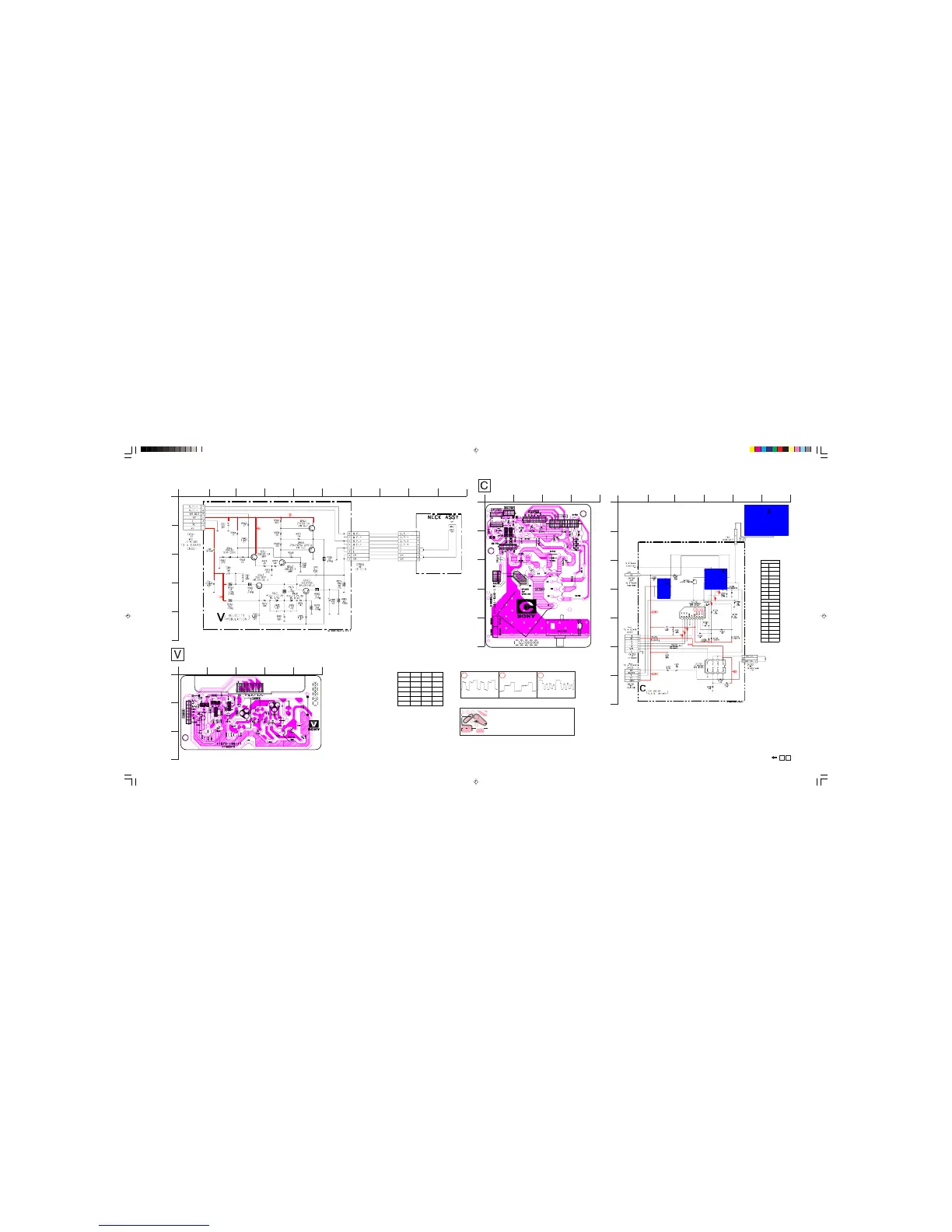
C BOARD WAVEFORMS
C BOARD SCHEMATIC DIAGRAM
NOTE:
Portions of the circuit marked as shown are high
voltage areas. Use care to prevent electric shocks
during inspection or repair.
A
B
C
D
E
A
B
C
V BOARD SCHEMATIC DIAGRAM
KV-24FV10/25FV10/25FV10C
1 2 3
132.8V p-p (H) 135.9V p-p (H) 140.6V p-p (H)
IC1707
PIN VOLT
13.8
24.5
34.5
40
56.1
66.1
76.1
89.0
IC1751
PIN VOLT
12.3
22.2
32.1
40
53.7
6 205.0
7 145.0
8 141.0
9 132.0
All volta ges are in V
C BOARD
IC VOLTAGE LIST
V BOARD TRANSISTOR
VOLTAGE LIST
V C Boards
A
B
C
D
E
853 5 CV Boards.p65 3/5/99, 12:10 PM1
 Loading...