33
SECTION 1
DIAGRAMS
1-1. NOTE FOR PRINTED WIRING BOARDS AND SCHEMATIC DIAGRAMS
Note on Printed Wiring Board:
• X : parts extracted from the component side.
• b : Pattern from the side which enables seeing.
• Indication of transistor.
B
These are omitted.
CE
Q
Note on Schematic Diagram:
• All capacitors are in µF unless otherwise noted. pF: µµF
50 WV or less are not indicated except for electrolytics
and tantalums.
• All resistors are in Ω and
1
/
4
W or less unless otherwise
specified.
• 2 : nonflammable resistor.
• C : panel designation.
• U : B+ Line.
• V : B– Line.
• Voltages are dc with respect to ground under no-signal
conditions.
no mark : AUDIO
• Voltages are taken with a VOM (input impedance 10 MΩ).
Voltage variations may be noted due to normal produc-
tion tolerances.
• Abbreviation
CND : Canadian model
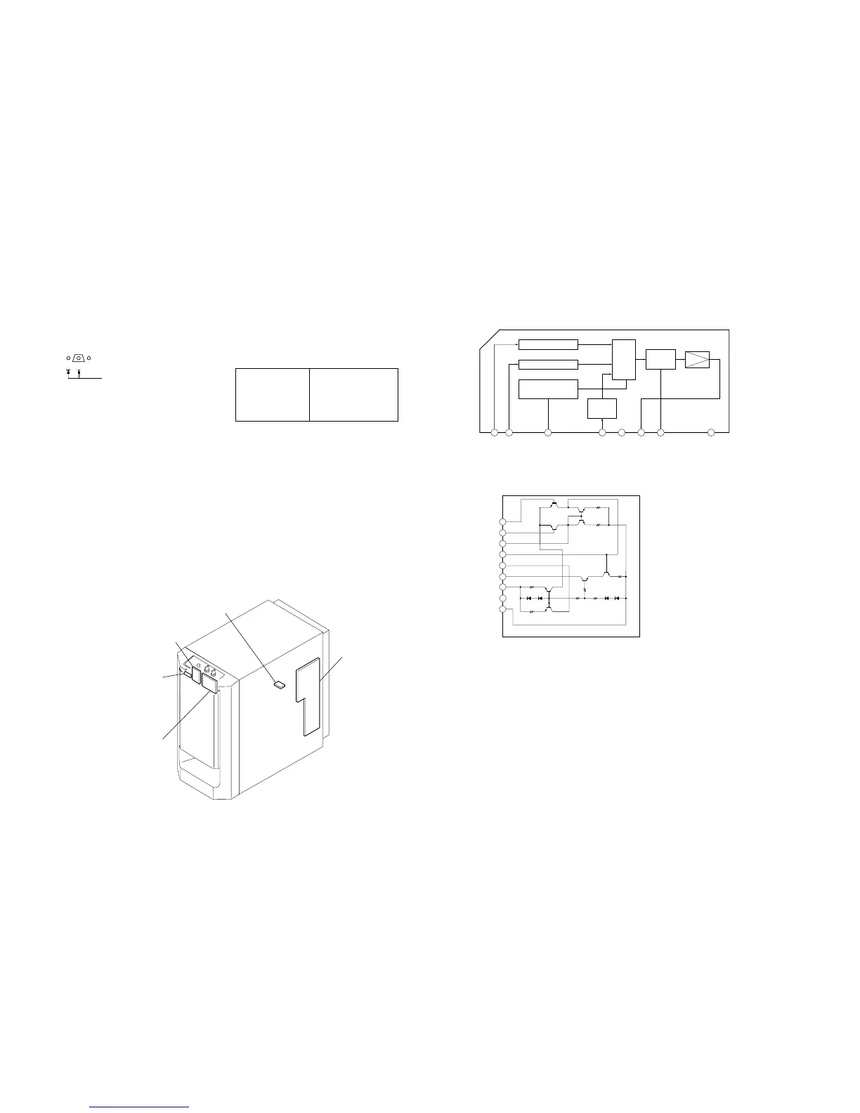
• Circuit Boards Location
SA-WMS315
• IC Block Diagrams
IC302 uPC1237H
IC301 STK350-230
1 2 3 4 5 6 7 8
OVER LOAD DET
F/F
OFFSET DET
LATCH/
AUTORESET
V
CC ON
MUTE
AC OFF
DET
V
CC
Note:
The components identi-
fied by mark 0 or dotted
line with mark 0 are criti-
cal for safety.
Replace only with part
number specified.
Note:
Les composants identifiés par
une marque 0 sont critiques
pour la sécurité.
Ne les remplacer que par une
piéce portant le numéro
spécifié.
POWER board
POWER SWITCH board
LED board
CONTROL board
MAIN boar
 Loading...