4
SECTION 3
DIAGRAMS
THIS NOTE IS COMMON FOR PRINTED WIRING
BOARDS AND SCHEMATIC DIAGRAMS.
(In addition to this, the necessary note is printed
in each block.)
For schematic diagrams.
Note:
• All capacitors are in µF unless otherwise noted. pF: µµF
50 WV or less are not indicated except for electrolytics
and tantalums.
• All resistors are in Ω and
1
/
4
W or less unless otherwise
specified.
•
f
: internal component.
• C : panel designation.
For printed wiring boards.
Note:
• X : parts extracted from the component side.
• Y : parts extracted from the conductor side.
•
a
: Through hole.
• b : Pattern from the side which enables seeing.
(The other layers' patterns are not indicated.)
• U : B+ Line.
• V : B– Line.
• H : adjustment for repair.
• no mark : FM
∗
: Can not be measured.
• Voltages are taken with a VOM (Input impedance 10 MΩ).
Voltage variations may be noted due to normal produc-
tion tolerances.
• Waveforms are taken with a oscilloscope.
Voltage variations may be noted due to normal produc-
tion tolerances.
• Circled numbers refer to waveforms.
• Signal path.
F : FM
J : CD
d : TAPE
G : REC (TAPE/MD)
j : MD
• Abbreviation
MY : Malaysia model.
SP : Singapore model.
HK : Hong Kong model.
KR : Korea model.
AED : North European model.
• Indication of transistor
C
These are omitted
EB
Q
C
These are omitte
EB
Note:
The components identified by mark 0 or
dotted line with mark 0 are critical for
safety.
Replace only with part number specified.
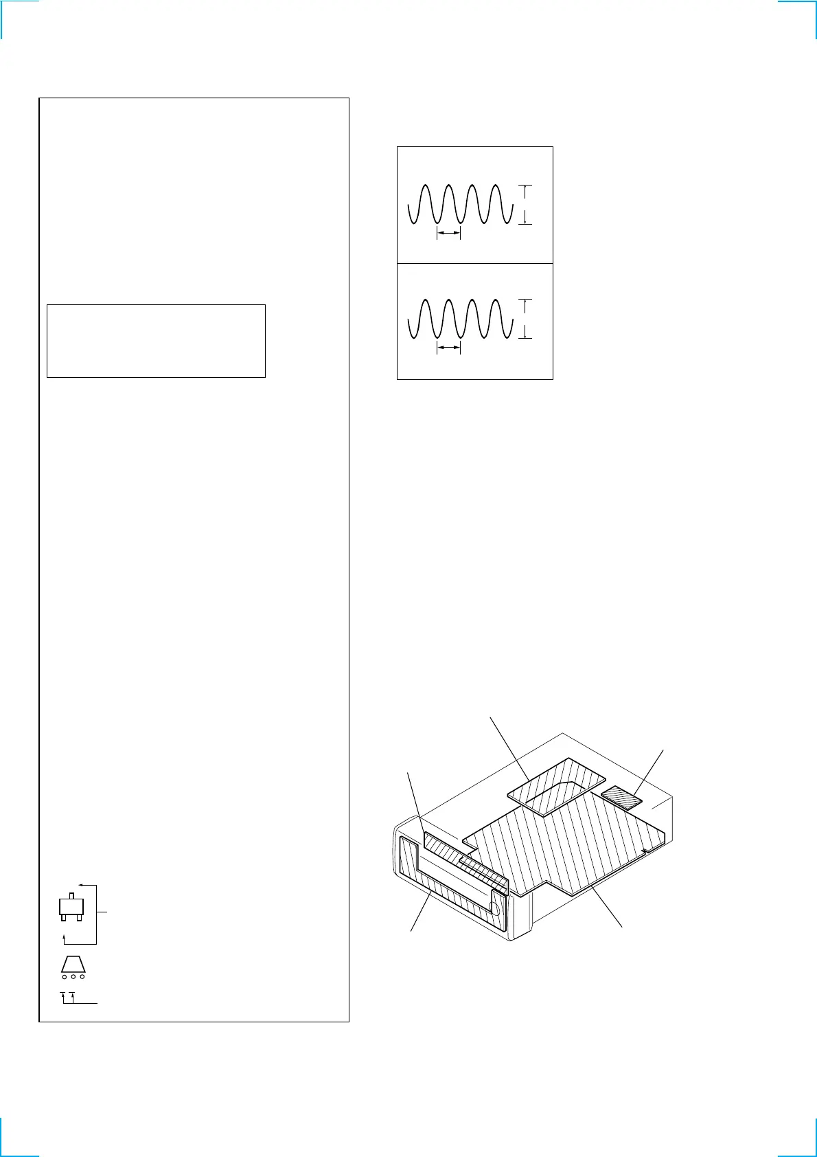
1
IC701 qa XCOUT
2
IC701 qd XOUT
30.5µsec
100nsec
2.7Vp-p
4.6Vp-p
• WAVEFORMS
– MAIN BOARD –
MAIN board
PANEL board
LED board
PIN JACK boar
tuner unit (FM/AM)
3-1. CIRCUIT BOARDS LOCATION
www.freeservicemanuals.info