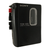
TCS-30D
– 15 – – 16 –
6-3. SCHEMATIC DIAGRAM • See page 17 for IC Block Diagrams.
Note on Schematic Diagram:
• All capacitors are in µF unless otherwise noted. pF: µµF
50 WV or less are not indicated except for electrolytics
and tantalums.
• All resistors are in Ω and
1
/
4
W or less unless otherwise
specified.
• C : panel designation.
• U : B+ Line.
• H : adjustment for repair.
• Total current is measured with no cassette installed.
• Power voltage is dc 3 V and fed with regulated dc power
supply from battery terminal.
• Voltages are dc with respect to ground under no-signal
conditions.
no mark : PB
( ) : REC
• Voltages are taken with a VOM (Input impedance 10 MΩ).
Voltage variations may be noted due to normal production
tolerances.
• Signal path.
E : PB
a : REC
N : MIC