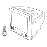
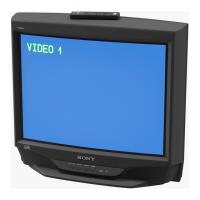
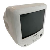
KV-PG14P40/PG14L70/PG14L70/H
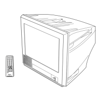
RM-952
– 3 –
TABLE OF CONTENTS
SELF DIAGNOSTIC FUNCTION ................................... 4
1. GENERAL ................................................................. 7
2. DISASSEMBLY
2-1. Rear Cover Removal ............................................... 10
2-2. Speaker Removal .................................................... 10
2-3. Chassis Assy Removal ............................................ 10
2-4. Service Position ...................................................... 10
2-5. Terminal Bracket Removal ..................................... 10
2-6. Replacement Of Parts ............................................. 10
2-6-1. Replacement Of Light Guide ....................... 10
2-6-2. Replacement Of Power Button .................... 10
2-7. Picture Tube Removal ............................................. 11
3. SET-UP ADJUSTMENTS
3-1. Beam Landing ......................................................... 12
3-2. Convergence ............................................................ 13
3-3. Focus Adjustment.................................................... 15
3-4. G2 (SCREEN) and white balance adjustments ...... 15
4. CIRCUIT ADJUSTMENTS
4-1. Adjustment With Commander ................................ 16
4-2. Adjustment Method ................................................ 16
4-3. Picture Quality Adjustment .................................... 21
4-4. Deflection Adjustment ............................................ 21
4-5. A Board Ajustment After IC003 (MEMORY)
Replacement ............................................................ 21
4-6. Picture Distortion Adjustment ................................ 22
Section Title Page
Section Title Page
5. DIAGRAMS
5-1. Block Diagram ........................................................ 23
5-2. Circuit Boards Location .......................................... 25
5-3. Schematic Diagram ................................................. 26
(1) Schematic Diagram of A Board ........................ 27
(2) Schematic Diagram of C Board ........................ 29
5-4. Voltage Measurement ............................................. 31
5-5. Waveforms .............................................................. 33
5-6. Printed Wiring Boards and Parts Location ............. 34
5-7. Semiconductors ....................................................... 37
6. EXPLODED VIEWS
6-1. Picture tube and Chassis ......................................... 39
7. ELECTRICAL PARTS LIST.................................... 40