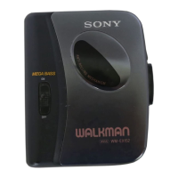
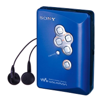
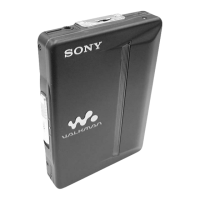
WM-EX910
– 17 –
– 18 –
– 19 –
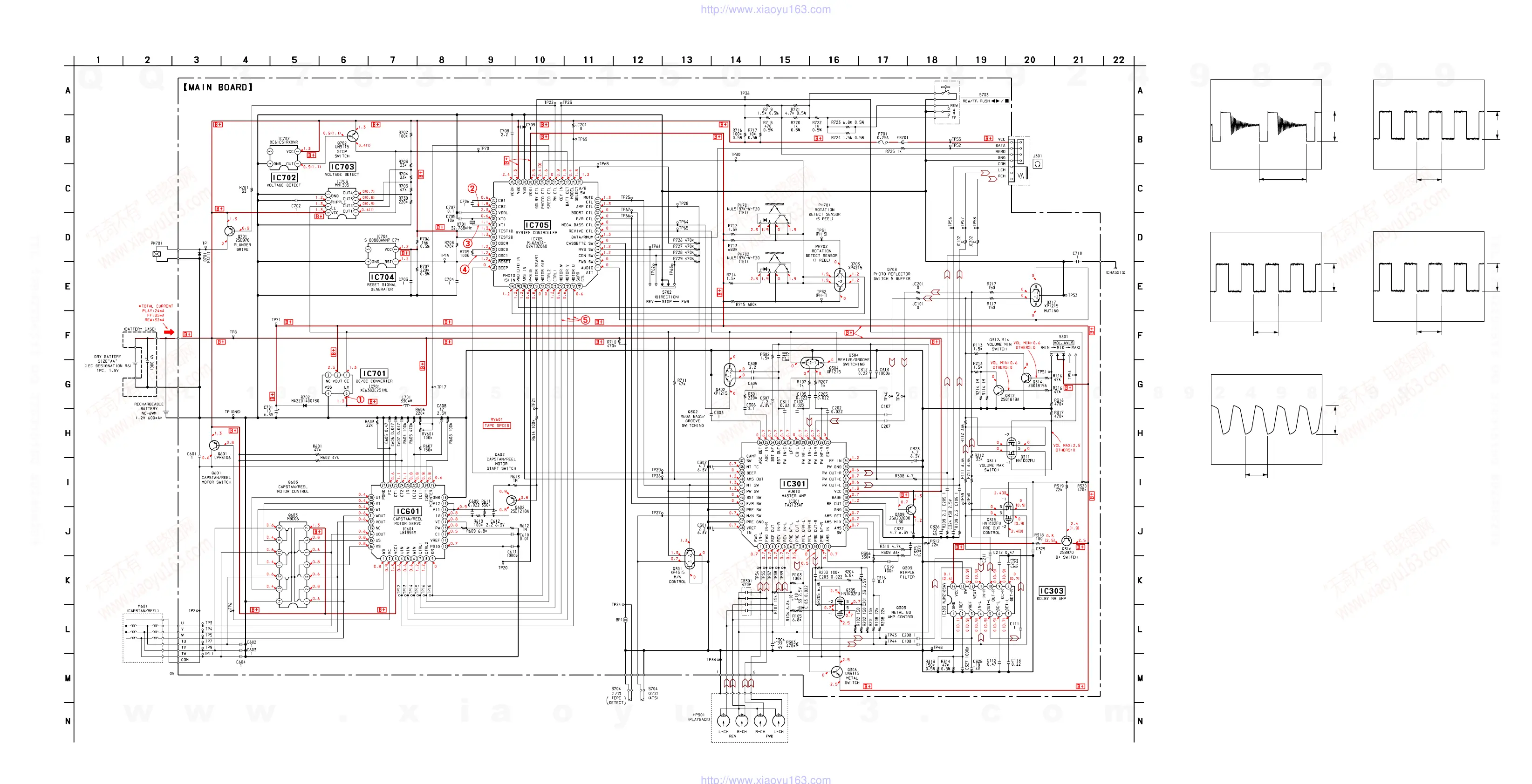
6-3. SCHEMATIC DIAGRAM • See page 20 for IC Block Diagrams.
• Waveforms
1 IC701 5 (LX)
1 V/DIV, 10 µs/DIV
2 IC705 wh (CB2)
500 mV/DIV, 20 µs/DIV
Note on Schematic Diagram:
• All capacitors are in µF unless otherwise noted. pF: µµF
50 WV or less are not indicated except for electrolytics
and tantalums.
• All resistors are in Ω and
1
/
4
W or less unless otherwise
specified.
• % : indicates tolerance.
• C : panel designation.
• A : B+ Line.
• U : B+ Line.
• H : adjustment for repair.
• Power voltage is dc 1.3 V and fed with regulated dc power
supply from battery terminal.
• Voltages and waveforms are dc with respect to ground
under no-signal conditions.
no mark : PLAY
( ) : STOP
[ ] : DOLBY NR ON
• Voltages are taken with a VOM (Input impedance 10 MΩ).
Voltage variations may be noted due to normal produc-
tion tolerances.
• Waveforms are taken with a oscilloscope.
Voltage variations may be noted due to normal produc-
tion tolerances.
• Circled numbers refer to waveforms.
• Signal path.
E : PLAY
3 IC705 wl (XT1)
1 V/DIV, 20 µs/DIV
4 IC705 ef (OSC1)
1 V/DIV, 1 µs/DIV
5 IC705 rg (MOTOR W), rh (MOTOR V),
rj (MOTOR U)
500 mV/DIV, 2 ms/DIV
3 Vp-p
3
µ
s
2.4 Vp-p
1.8
µ
s
1.3 Vp-p
6.6 ms
w
w
w
.
x
i
a
o
y
u
1
6
3
.
c
o
m
Q
Q
3
7
6
3
1
5
1
5
0
9
9
2
8
9
4
2
9
8
T
E
L
1
3
9
4
2
2
9
6
5
1
3
9
9
2
8
9
4
2
9
8
0
5
1
5
1
3
6
7
3
Q
Q
TEL 13942296513 QQ 376315150 892498299
TEL 13942296513 QQ 376315150 892498299
http://www.xiaoyu163.com
http://www.xiaoyu163.com
 Loading...