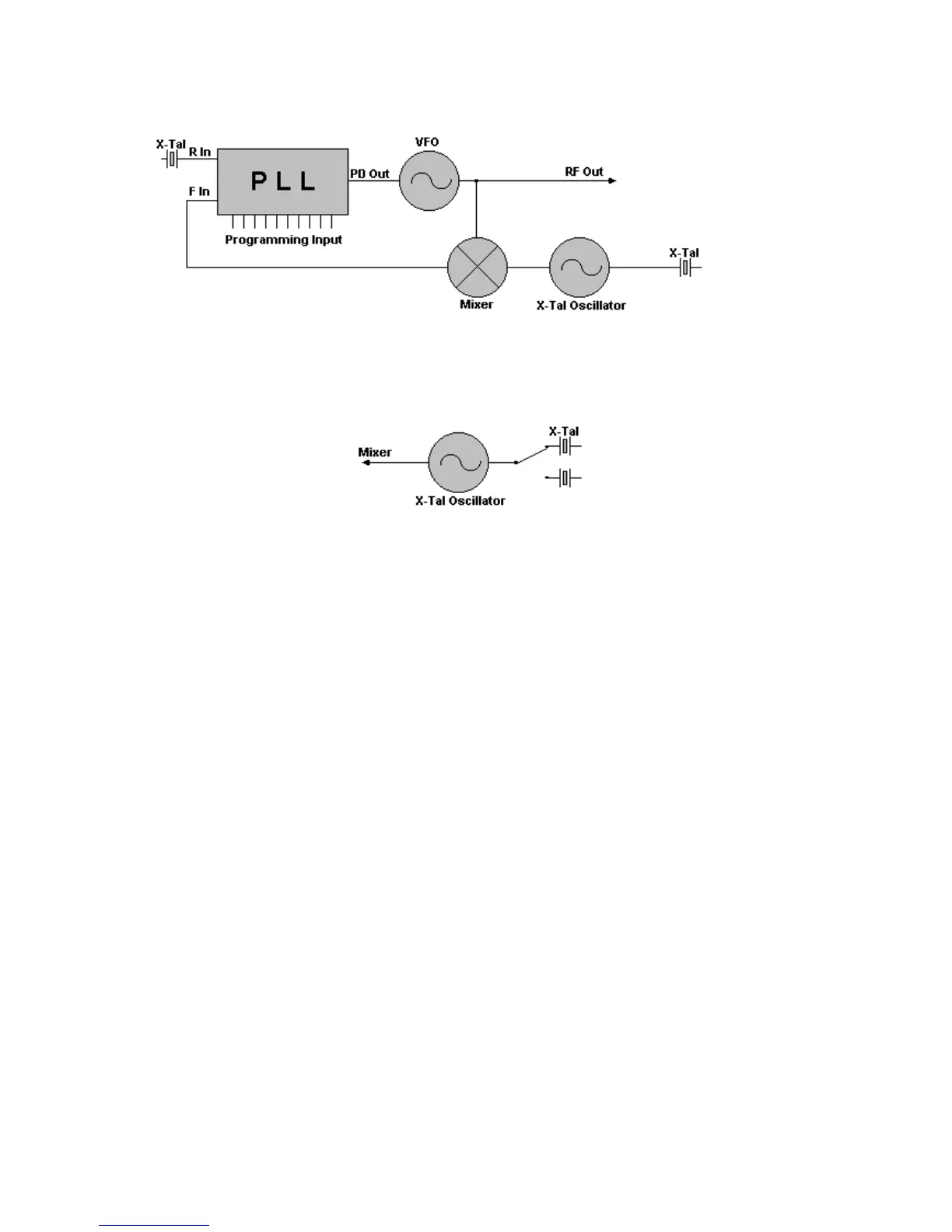
Down-converting of the frequency to the divider
This PLL Circuit use a Mixer and a X-Tal Oscillator to convert the output frequency f
OUT
to the f
IN
to
the PLL Circuit.
The X-Tal frequency is f
XTAL
= f
OUT
- f
IN
The output frequency can be changed by changing the mixing-xtal or add a new mixing-xtal to the
oscillator.
Pin
Name
Description
1
VDD Positive Power Supply
2
F in VCO Oscillator Input
3
RI
Reference Oscillator Input (10.240MHz)
4
FS HIGH=10kHz - LOW=5kHz
5
PD VCO Voltage Out
6
LD
Loop Detected - HIGH=Locked LOW=Unlocked
7
P8 Programmable input (Binary)
8
P7 Programmable input (Binary)
9
P6
Programmable input (Binary)
10
P5 Programmable input (Binary)
11
P6 Programmable input (Binary)
12
P3 Programmable input (Binary)
13
P2 Programmable input (Binary)
14
P1 Programmable input (Binary)
15
P0 Programmable input (Binary)
16
Vss Ground
Explanation of pin function terms
V
CC
or V
DD
This is the +DC supply voltage which actually provides the operating power to the chip,
and is generally in the range of 4-8 volts.
GND or V
SS
This is the DC power ground connection for the above. NOTE: A chip may be found to
have one or more of its functional pins tied to either of the above sources. This may be done to enable
a specific function by connecting that function to a ''1'' or ''0'' , or to prevent an unused function pin
from ''floating'' unconnected to prevent a possible change in its logic state.
RI Reference Oscillator input. This is where the (usually) 10.240 MHz crystal is connected. Crystal
pins sometimes called ''X'' by the manufacturer.
RO Reference Oscillator output. In most chips the crystal is simply connected across RI and RO
because the chip has a built-in oscillator circuit which only requires some external capacitors. However
some chips such as the PLL02A don't have the built-in oscillator; thus there is no RO pin and an active
transistor oscillator is required externally which connects to RI.
 Loading...