47
Chapter 2: Installation
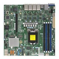
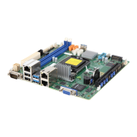
SGPIO Headers
There is one Serial Link General Purpose Input/Output (I-SGPIO1) header located on the
motherboard. The SGPIO header is used to communicate with the enclosure management
chip on the back panel.
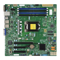
X11SCL-IF
REV:1.01
1
BIOS LICENSE
BAR CODE
+
DESIGNED IN USA
Intel
i210
Intel
C242
ASpeed
AST2500
JPL1
FANA
JLED1
JPME2
JWD1
JPL2
JPG1
JSTBY1
USB2/3
CPU SLOT1 PCI-E 3.0 X16
B1
JL1
LED4
M.2-H
MH5
LED2
JUIDB1
JD1
LED5
SP1
VGA
JTPM1
CPU
USB6/7(3.0)
LAN1/2
USB8(3.0)
JBT1
USB4/5
(3.0)
I-SATA0
JSD2
I-SATA1
JSD1
USB0/1
IPMI LAN
I-SATA2
I-SATA3
X NMI
LED
PWRHDD
LED1
NIC
2
NICUID
LED
PS
FAIL
RST
PWR
ON
JF1
DIMMB1
DIMMA1
FAN2
FAN1
LED3
JPW1
FAN3
I-SGPIO1
JPW2
JF1
COM1
1. I-SGPIO1 Header
2. JSD1 (DOM PWR)
3. JSD2 (DOM PWR)
1
Disk-On-Module Power Connector
Two power connectors for SATA DOM (Disk-On-Module) devices are located at JSD1 and
JSD2. Connect appropriate cables here to provide power support for your Serial Link DOM
devices.
DOM Power
Pin Denitions
Pin# Denition
1 5V
2 GND
3 GND
3
2
SGPIO Header
Pin Denitions
Pin# Denition Pin# Denition
1 NC 2 NC
3 GND 4 DATA Out
5 Load 6 GND
7 Clock 8 NC
NC = No Connection
 Loading...