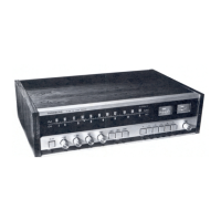
Do you have a question about the TANDBERG TR 2025 and is the answer not in the manual?
Instructions for cleaning and lubricating push button switches for trouble-free action.
Procedures for disassembling various types of switches: Independent, Interlocking, and Independent.
Steps to remove the cabinet top panel and side panels.
Procedure for removing the dial holder, including meter and lamp connections.
Steps to remove the front plate, including knobs and front strip.
Guidance on applying thermal compound to mica washers for output transistors.
Instructions for removing, fitting, and servicing the cord drive mechanism.
Procedure for setting the dial pointer after cord drive assembly.
Detailed steps for aligning the FM tuner using generator and oscilloscope.
Procedures for aligning the stereo decoder with a stereo generator.
Important notes regarding FM alignment, filter replacement, and decoder alignment.
Alternative alignment procedures when specific test equipment is unavailable.
Component layout for the FM-IF and decoder board using TCA 4500 IC.
Steps for fault finding in the FM tuner, including tuner lock and AGC lead.
Schematic diagram for the FM tuner section (Board A1).
Schematic diagram for the FM-IF and decoder board (MC 1310P IC).
Solder-side view of the FM-IF and decoder board (TCA 4500 IC).
Troubleshooting steps for the FM tuner, including tuner lock and AGC lead.
Component layout for the FM tuner section (Board A1).
Component layout for the FM-IF and decoder board (MC 1310P IC).
Detailed schematic diagram of the FM tuner board (A1).
Schematic diagram of the FM-IF and stereo decoder board (A2).
Diagram illustrating signal path voltages at various points in the circuit.
Schematic diagram for the decoder circuit using TCA 4500 IC.
Schematic diagram for the decoder circuit using MC 1310P IC.
Procedure for measuring quiescent current in the left channel AF output.
Procedure for measuring quiescent current in the right channel AF output.
Circuit diagram for the RIAA and input amplifier stages.
Circuit diagram for the power amplifier section.
Component layouts for the power amplifier (left and right channels).
Component layout for the RIAA/input amplifier stages.
Component layout for the AF output stages.
Procedure for adjusting quiescent current in the amplifier channels.
Component layout and wiring for the preamplifier board (A6).
Component layout and wiring for the power amp and input circuit board (A5).
Details of tone control components and their layout on the preamp board.
Circuit diagram and component layout for the pointer dial light board.
Information about mains transformer part numbers and wiring configurations.
Circuit diagram for the power amp and input circuit board (A7).
Schematic for a section of the preamplifier board.
Solder-side view of the preamplifier board (A6).
Solder-side view of the power amp and input circuit board (A5).
Diagrams and specifications for connecting FM aerials.
Details on DIN plugs for connecting record players, tape recorders, and headphones.
Useful data including input sensitivity, impedance, and power consumption.
| Power output | 25 watts per channel into 8Ω (stereo) |
|---|---|
| Frequency response | 20Hz to 20kHz |
| Input sensitivity | 2.5mV (MM), 150mV (line) |
| Output | 150mV (line) |
| Speaker load impedance | 4Ω to 16Ω |
| Tuning range | FM: 87.5-108 MHz |
| Signal to noise ratio | 85dB (line) |