Do you have a question about the Technics SE-A2000 and is the answer not in the manual?
Details on power consumption, power supply, dimensions, and weight.
Step-by-step instructions for replacing the fuse in the power plug.
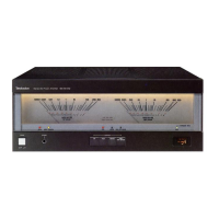
The main power switch for the amplifier unit.
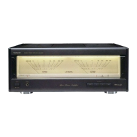
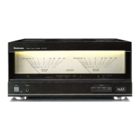
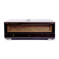
Indicators showing the operating condition: Voltage Control and Current Drive.
Port for connecting headphones for private listening.
Displays the output power in watts, with adjustments for speaker impedance.
Allows selection of connected speakers (A, B, or A+B) and indicates status.
Instructions for connecting speaker wires to terminals A and B.
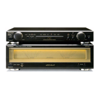
How to connect the amplifier to a control amplifier using a stereo cable.
Instructions for setting the voltage selector for different regions.
Guidance on connecting the power cord, referencing safety cautions.
Procedure for using headphones, including volume adjustment.
Explanation of the advanced Class AA circuit using MOS FETs and bipolar transistors.
Details on the transformer design for reduced noise and improved performance.
Description of independent left/right channels and high-performance power supplies.
Description of the large-sized power meters and operation indicators.
Details on the electronic switches and gold-clad contacts for speaker selection.
Information on the vibration-proof design and rigid chassis construction.
Step-by-step guide to removing the left and right side panels.
Instructions for removing the main cabinet assembly.
Procedure for removing the left and right cabinet ornaments.
Guide to removing the front panel assembly, including connectors.
Instructions for removing the power switch printed circuit board.
Procedure for removing the LED printed circuit board.
Steps to remove the speaker selector and logic printed circuit board.
Instructions for removing the speaker switch printed circuit board.
Guide for removing the lamp printed circuit boards.
Procedure for removing the lamp house assembly.
Instructions for removing the front transparent glass panel.
Steps to remove the front panel meter assembly.
Procedure for removing the left and right sub radiating plates.
Instructions for removing the left and right voltage control amplifier PCBs.
Guide to removing the internal pre-shield case.
Instructions for removing the right side angle component.
Procedure for removing the left side angle and fuse PCB.
Steps to remove the relay printed circuit board.
Instructions for removing the latch mechanism.
Procedure for removing the left and right twin capacitor assemblies.
Instructions for removing the left and right power transformer units.
Steps to remove the left and right current drive amplifier printed circuit boards.
Guide for removing the power transistors, including mounting tips.
Instructions for removing the left and right speaker terminal PCBs.
Steps to remove the input terminal printed circuit board.
Procedure for removing the AC inlet printed circuit board.
Instructions for checking and replacing parts on specific PCBs.
Procedure for checking and replacing parts on the speaker selector/logic PCB.
Instructions for checking and replacing parts on voltage control amplifier PCBs.
Procedure for adjusting the idle current of the voltage control amplifier.
Procedure for adjusting the idle current of the current drive amplifier.
Steps to calibrate the power meters to indicate correct output wattage.
Schematic of input, voltage amp, meter amp, muting, and protector circuits.
Schematic of speaker selector and logic control circuits.
Schematic of the Clamp (1) circuit.
Schematic of the Clamp (2) circuit.
Schematic of the power supply section.
Schematic of the LED indicator circuits.
Schematic of the left channel voltage control amplifier.
Schematic of the right channel voltage control amplifier.
Schematic of the left channel current drive amplifier.
Schematic of the relay control circuits.
Schematic of the power switch control circuit.
Schematic of the speaker output circuits.
Schematic of the AC power inlet circuit.
Diagram showing the layout of the Input Terminal PCB.
Diagram showing the layout of the Speaker Selector/Logic PCB.
Diagram showing the layout of the Voltage Control Amp (L) PCB.
Diagram showing the layout of the Current Drive Amp (L) PCB.
Diagram showing the layout of the Speaker Switch PCB.
Diagram showing the layout of the LED PCB.
Diagram showing the layout of the Voltage Control Amp (R) PCB.
Diagram showing the layout of the Current Drive Amp (R) PCB.
Diagram showing the layout of the Relay PCB.
Diagram showing the layout of the Lamp (1) PCB.
Diagram showing the layout of the Speaker Terminal (R) PCB.
Diagram showing the layout of the Fuse PCB.
Diagram showing the layout of the AC Inlet PCB.
Diagram of the Power Source PCB, specific to the (G) area.
Diagram of the Voltage Adjustment PCB.
Diagram of the Fuse (1) PCB.
Diagram of the Fuse (2) PCB.
Wiring diagram for the Input Terminal PCB.
Wiring diagram for the Speaker Selector/Logic PCB.
Wiring diagram for the Voltage Control Amp (L) PCB.
Wiring diagram for the Lamp (2) PCB.
Wiring diagram for the Speaker Switch PCB.
Wiring diagram for the LED PCB.
Wiring diagram for the Current Drive Amp (L) PCB and transformer connection.
Wiring diagram for the Voltage Control Amp (R) PCB.
Wiring diagram for the Current Drive Amp (R) PCB.
Wiring diagram for the Relay PCB.