Do you have a question about the Technics SH-8066 and is the answer not in the manual?
Details frequency response, output voltage, input sensitivity, and harmonic distortion.
Covers band level controls, center frequencies, and microphone sensitivity.
Details the technical specifications of the microphone supplied with the unit.
Outlines the procedure for testing insulation resistance for safety.
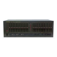
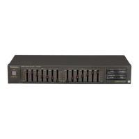
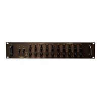
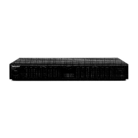
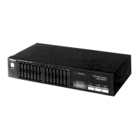
Identifies and explains the function of each control on the front panel.
Describes the various input and output jacks on the rear panel.
Explains display operation, memory features, and pink noise generator.
Guides on measuring frequency response and manual equalization control.
Explains how to save custom equalization settings into memory.
Explains the design and function of the semi-conductive inductor BPF circuit.
Details the power supply circuits for different regions and their components.
Illustrates the physical arrangement of internal and external parts.
Lists part numbers for integrated circuits, transistors, and diodes.
| Type | Stereo Equalizer |
|---|---|
| Frequency Bands | 10 |
| Total Harmonic Distortion | 0.005% |
| Signal-to-Noise Ratio | 100dB |
| Dimensions | 420 x 300 x 100 mm |
| Weight | 3.5 kg |
| Frequency response | 20 Hz - 20 kHz |
| Control Range | ±12 dB |
| Frequency Range | 20 Hz - 20 kHz |
| Output Impedance | 600 Ω |
| Frequency Bands (Hz) | 1k, 2k, 4k, 8k, 16k |