Do you have a question about the Technics SH-9010 and is the answer not in the manual?
Specifies the rated and maximum output voltage and impedance of the unit.
Details the total harmonic distortion level at the rated output.
Provides the input sensitivity and impedance specifications.
Outlines the frequency response across all band-level controls.
Specifies the gain levels.
Details the signal-to-noise ratio measured using the IHF standard.
Details the signal-to-noise ratio measured using the DIN 45 500 standard.
Describes the adjustment range for band-level controls.
Details the adjustment range for center-frequency controls.
Specifies the range and variability of the bandwidth control.
Lists the standard center frequencies for the equalizer bands.
Indicates the power consumption of the unit.
Specifies the voltage requirements for the power supply.
Provides the physical dimensions (width, height, depth) of the unit.
States the weight of the unit.
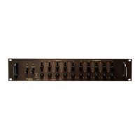
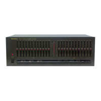
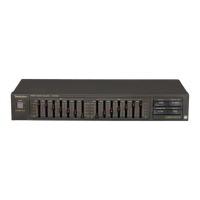
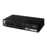
Identifies controls visible on the front panel of the unit.
Highlights key components visible on the inside of the unit.
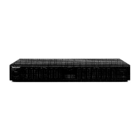
Details connections and selectors on the rear panel.
Explains how to use the frequency level controls for adjustment.
Describes the function and adjustment of center frequency controls.
Details the operation and adjustment of the bandwidth (Q) controls.
Details how to use frequency level controls for adjustment.
Provides the definition and formula for the Q factor.
Describes the adjustment range for center frequency controls.
Details the construction and operation of the band-pass filter circuits.
Explains the operational section that forms the peak and dip frequency response.
Instructions for adjusting the voltage regulation circuit.
Procedure for adjusting the DC unbalanced voltage.
Details the procedure for adjusting individual frequency gain.
Diagram of the input buffer circuitry.
Diagram of the adder circuitry.
Diagram of the band-pass filter circuits for different frequencies.
Diagram of the voltage regulator circuitry.
Critical safety information regarding component replacement.
Provides important notes and explanations related to the schematic diagram.
Layout of the input buffer circuitry on the PCB.
Layout of the adder/subtracter circuitry on the PCB.
Layout of the band-pass filter circuits on the PCB.
Layout of the voltage regulator circuitry on the PCB.
Identifies specific points on the PCB for alignment procedures.
Shows the internal block diagram of the integrated circuit.
Critical safety information regarding replacement of specific components.
List of replacement integrated circuits with part numbers and descriptions.
List of replacement transistors with part numbers and descriptions.
List of replacement diodes with part numbers and descriptions.
List of replacement transformers with part numbers.
List of replacement resistors with part numbers and specifications.
List of replacement switches with part numbers and types.
List of replacement relays with part numbers.
List of replacement cabinet and chassis components.
Illustrates the assembly of the unit with numbered parts.
Details parts visible and accessible from the front of the unit.
Details components and parts located on the rear panel.
List of replacement capacitors with part numbers and specifications.
List of replacement lamps with part numbers.
List of replacement fuses with part numbers.
List of replacement relays with part numbers.
List of packing materials and components.
Details of packing materials and components for different regions.
List of included accessories and their regional availability.
| Brand | Technics |
|---|---|
| Model | SH-9010 |
| Category | Stereo Equalizer |
| Language | English |