Do you have a question about the Technics SU-V6 and is the answer not in the manual?
Details amplifier performance: RMS power output, harmonic distortion, dynamic headroom, and damping factor.
Covers input sensitivity, frequency response, S/N ratios, tone controls, filters, and general unit specs.
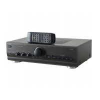
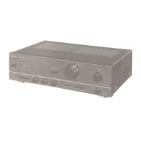
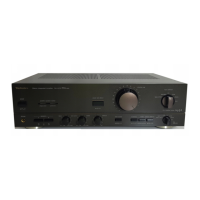
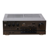
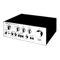
Identifies front panel controls: mode selectors, input, tone, operation, loudness, filters, and indicators.
Details rear panel terminals: inputs, outputs, speaker connections, and AC outlets.
Explains the operation of the synchronous bias circuit and its role in preventing switching distortion.
Outlines the procedure for checking the proper operation of the synchronous bias circuit.
Compares Class B and Class A amplification methods against the unit's New Class A approach.
Details the New Class A method, highlighting its benefits for sound quality and output power.
Details the settings, connections, and steps for DC balance and ICQ adjustments.
Provides guidance on disassembling the unit, including removing power transistors and switch bands.
Shows the layout for the power amplifier drive and synchronous bias circuits (PCB A).
Illustrates the printed circuit board layout for the pre-drive circuit (PCB D).
Presents the complete schematic diagram of the SU-V6 amplifier's circuitry.
Highlights key components and their locations within the schematic diagram.
Details the layout for the power amplifier drive and synchronous bias circuits (PCB B).
Shows the printed circuit board layout for the pre-drive circuit (PCB C).