The address command may precede a data command or query to identify the instrument bus location as part of the
same message.
Errors related to ADDR and DATA commands:
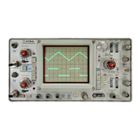
Maintenance—492/492P Service Vol. 1 (SN B030000 & up)
Error
41
42
ADDR and DATA COMMAND
ADDR/DATA argument invalid
ADDR not compatible for DATA command
Instrument Bus Registers
Registers provide the link between the instrument bus
and microcomputer-controlled functions. The registers are
defined here in order according to the number of the dia
gram where the register appears. The definitions are pro
vided to help in constructing DATA commands (see above)
and interpreting responses to DATA queries.
bandwidth. When DB7 equals 0, it steers DB6 through DBO
to select the amount of gain added in the VR section and the
band-leveling gain (gain adjustment related to front-end re
sponse in each band). These two functions are addressed
and set together by the same data byte, although they are
broken into two portions of the table below to show the
portions of the data byte that form the codes for the two
functions.
m
The data is presented here as binary. In some cases the
data occupies the entire register width, as does a value in
digital storage, for instance. In other cases, a single bit or
group of bits in the register conveys a code. The upper five
bits in the sweep rate and mode register indicate the sweep
time/division, for instance. The meaning of the data is not
fully defined here; refer to the description of the circuit mod
ule in Section 5 for details.
To use the binary data and codes presented here with
the DATA command and query presented above, you must
convert binary to hexadecimal. This takes three steps:
1) group the lower four bits and the upper four bits (break
the data byte in half);
2) convert each group of four bits to a hex. digit. Hex. digits
range from 0 to F in this sequence: 0123456789ABCDEF;
3) group the two hex. digits together, keeping their respec
tive places—upper and lower.
For example, binary code 01001011 would be trans
formed by:
1) 01001011 = 0100 1011
2) 0100 = 4 and 1011 = B (8 + 0+2 + 1=B)
3) 4 and B make the two-digit hex. number 4B.
Variable Resolution Mother Board #2 (refer to dia
gram 19). There are two variable resolution registers that
the microcomputer writes to, although both are addressed
at 3F (see Table 4-5). The data MSB steers the other bits
that are defined into the desired register. When DB7 equals
1, it steers DBO through DB2 to select the resolution
Table 4-5
VARIABLE RESOLUTION DATA REGISTER (3F)
Resolution Bandwidth DB7 = 1
DB7
DB2
DB1 DBO
Selects
1
0 0
1
1 MHz
1
0
1 0
100 kHz
1
0
1 1
10 kHz
1
0
0
1
1 kHz
1
1 0
1
100 Hz
1
1
1
0
For future use
Gain, Leveling DB7=0
DB7
DB6 DB5
DB4
DB3
Leveling
0
0 0
0 0
Band 1
0
0
1 0
0
Band 2
0 0 0
1 0
Band 3
0 0
1 1 0
Band 4
0
0 0
0
1
Band 5
0
0
1 0
1 Band 6
0 0 0
1
1 Band 7
0 0
1
1 1
Band 8
0 1 0 0
0
Band 9
0
1 1 0 0
Band 10
DB7
DB2 DB1 DBO
Gain
0 0 0 0
OdB
0
0 0
1
10 dB
0
1
0 0
20 dB
0
1
0
1
30 dB
0
1 1
1
40 dB
REV JUN 1983
4-45
 Loading...