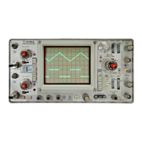
Theory of Operation—492/492P Service Vol. 1 (SN B030000 & up)
Since the two buffers are nearly identical, only the 2nd
Converter buffer is described. Gain is provided by a single
"l common-emitter transistor (Q1011). Printed elements pro
vide input and output impedance matching. Out-of-band
damping is provided by R1011 in series with a 1/4
wavelength shorted stub. Dc is blocked by C1014 and
C1011. A 1/4 wavelength open stub is used at the output to
reflect one of the 2nd Converter’s image frequencies at
4254 MHz (the other buffer does not use nor need this
stub). Collector bias for Q1011 is provided through R1012,
L1011, the 1/4 wavelength shorted stub, and R1011. The
1/4 wavelength shorted stub is grounded through C2011
(C2011, C1013, and L1011 are also used for decoupling).
Collector voltage is determined by divider R1013 and
R2013; this controls the dc feedback to the collector-base
junction of Q1011. The bias network is decoupled from the
RF path by L1014. Diode CR2013 protects the base of
Q1011 from excessive reverse bias if the +12 volt supply
fails.
2200 MHz Reference Board
This circuit generates harmonics of the 100 MHz input.
The 22nd harmonic or 2200 MHz is used by the Reference
Mixer. The input 100 MHz signal is applied through a match
ing network (consisting of L1034, L1025, C1036, C1029,
and C1025) to a differential amplifier (Q1024 and Q2024).
The emitters of this amplifier are ac coupled through C2026,
reducing low frequency gain and ensuring balanced oper
ation. A snap-off diode (CR2014) is driven by the amplifier,
via transformer T2015, to generate multiple harmonics of
the 100 MHz signal including the 2200 MHz reference. The
output passes through a 3 dB attenuator, for isolation, to
the Reference Mixer circuit.
2200 MHz Reference Mixer
Signals from the 2200 MHz Reference circuit are filtered
by a printed 2200 MHz bandpass filter. Diodes CR1011 and
CR1012 are the switching elements of a single-balanced
mixer. The microstrip oscillator output is applied to CR1011
and through a 1/2 wavelength delay line to CR1012. The
delay line shifts the oscillator signal 180° so both diodes
switch together. Mixing the 2200 MHz with the oscillator
2182MHz signal produces the difference frequency of
18 MHz. This 18 MHz signal is fed through a 37 MHz
lowpass filter to the 14-22 MHz phaselock circuit. The
lowpass filter prevents unwanted products, such as 82 MHz
(product of 2100 MHz and 2182 MHz), from passing into the
phaselock circuit.
14-22 MHz Phaselock Board
This board contains regulated power supplies, a 14-
I 22 MHz (18 MHz nominal) voltage controlled oscillator with
linearizing circuitry, and a phase/frequency detector circuit.
Its main function is control of the 2182 MHz Microstrip Os
cillator. The entire circuit board is housed in a magnetic
shield to reduce spurious effects of external ac fields. All
power supply and control inputs enter the circuit board via
feedthrough capacitors in the housing wall. All connections
with the microwave circuitry are through feedthrough ca
pacitors C2200-C2204, in the floor of the housing.
The +15 V, -15 V, and + 9V inputs supply power to
operational amplifier type regulators that produce +12 V,
— 12 V, and +5.2 V outputs, respectively. A zener diode
(VR2021) serves as a stable —6.2 V reference for U2014B,
which regulates the -12 V supply through emitter-follower
Q2021. The —12 V supply, in turn, provides bias current for
VR2021. Diodes CR2015 and CR2018 protect the oper
ational amplifier output and Q2021 during supply shutdown.
Inverting amplifiers U2014A/Q1012 and U1015/Q1022 use
the — 12 V supply as a reference to produce the +12 V and
+ 5.2 V supplies, respectively.
The 2nd LO sweep and tune inputs are summed by dif
ferential amplifier U2063. Ground potential of the Span
Attenuator circuit is sensed through R2057 and subtracted
from the sweep signal to reduce effects of ground potential
variations. Provision is made for sensing the ground poten
tial of the Center Frequency Control circuit board through
R2059; however, the present interface requires that the
Fine Tune ground input be grounded to the 2nd LO assem
bly through W2059. Sweep and tune sensitivities are set by
selectable resistor R2063.
The combined sweep and tune signals, at the output of
U2063, are applied to a non-linear shaping circuit, the gain
of which varies as a function of input signal voltage. Output
voltage from the shaper circuit controls the bias of varactor
diode CR1075. This bias tunes the 14-22 MHz oscillator.
Non-linear tuning characteristics of the oscillator are com
pensated by reciprocal non-linearity in the shaper. As the
input voltage to non-inverting amplifier U1062B becomes
more positive, it successively exceeds the tap-point
voltages of a series of positive voltage dividers. Diodes in
U2051, connected to the divider tap points, are successively
forward biased to add increasing shunt conductance to the
amplifier’s feedback path. Feedback progressively de
creases and forward gain of the amplifier increases with
positive excursions. A similar amplifier, U1062A, uses nega
tive voltage dividers and the diodes in U1051 to increase the
gain progressively with negative voltage excursions. Out
puts of the two amplifiers are summed at R1068, which is
selected to match the gain shaping requirements of the 14-
22 MHz oscillator. One of the varactor bias resistors,
R1070, is also selected as part of the linearity adjustment.
The 14-22 MHz oscillator consists of a differential ampli
fier with transformer feedback. The emitters of the amplifier
transistors Q2073 and Q2078 are ac coupled through
REV AUG 1981
5-11
 Loading...