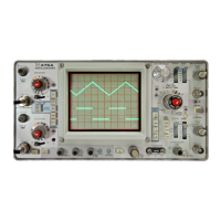
Theory of Operation—492/492P Service Vol. 1 (SN B030000 & up)
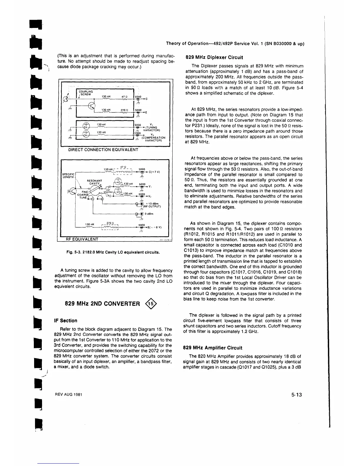
(This is an adjustment that is performed during manufac
ture. No attempt should be made to readjust spacing be
cause diode package cracking may occur.)
DIRECT CONNECTION EQUIVALENT
Fig. 5-3. 2182.0 MHz Cavity LO equivalent circuits.
A tuning screw is added to the cavity to allow frequency
adjustment of the oscillator without removing the LO from
the instrument. Figure 5-3A shows the two cavity 2nd LO
equivalent circuits.
829 MHz 2ND CONVERTER <^>
IF Section
Refer to the block diagram adjacent to Diagram 15. The
829 MHz 2nd Converter converts the 829 MHz signal out
put from the 1 st Converter to 110 MHz for application to the
3rd Converter, and provides the switching capability for the
microcomputer controlled selection of either the 2072 or the
829 MHz converter system. The converter circuits consist
basically of an input diplexer, an amplifier, a bandpass filter,
a mixer, and a diode switch.
829 MHz Diplexer Circuit
The Diplexer passes signals at 829 MHz with minimum
attenuation (approximately 1 dB) and has a pass-band of
approximately 200 MHz. All frequencies outside the pass-
band, from approximately 50 kHz to 2 GHz, are terminated
in 50 Ω loads with a match of at least 10 dB. Figure 5-4
shows a simplified schematic of the diplexer.
At 829 MHz, the series resonators provide a low-imped-
ance path from input to output. (Note on Diagram 15 that
the input is from the 1 st Converter through coaxial connec
tor P231.) Ideally, none of the signal is lost in the 50 Ω resis
tors because there is a zero impedance path around those
resistors. The parallel resonator appears as an open circuit
at 829 MHz.
At frequencies above or below the pass-band, the series
resonators appear as large reactances, shifting the primary
signal flow through the 50 Ω resistors. Also, the out-of-band
impedance of the parallel resonator is small compared to
50 Ω. Thus, the resistors are essentially grounded at one
end, terminating both the input and output ports. A wide
bandwidth is used to minimize losses in the resonators and
to eliminate adjustments. Relative bandwidths of the series
and parallel resonators are optimized to provide reasonable
match at the band edges.
As shown in Diagram 15, the diplexer contains compo
nents not shown in Fig. 5-4. Two pairs of 100Ω resistors
(R1012, R1015 and R1011 /R1012) are used in parallel to
form each 50 Ω termination. This reduces load inductance. A
small capacitor is connected across each load (C1010 and
C1013) to improve impedance match at frequencies above
the pass-band. The inductor in the parallel resonator is a
printed length of transmission line that is tapped to establish
the correct bandwidth. One end of this inductor is grounded
through four capacitors (C1017, C1016, C1019, and Cl 018)
so that dc bias from the 1 st Local Oscillator Driver can be
introduced to the mixer through the diplexer. Four capaci
tors are used in parallel to minimize inductance variations
and circuit Q degradation. A lowpass filter is included in the
bias line to keep noise from the 1 st converter.
The diplexer is followed in the signal path by a printed
circuit five-element lowpass filter that consists of three
shunt capacitors and two series inductors. Cutoff frequency
of this filter is approximately 1.2 GHz.
829 MHz Amplifier Circuit
The 820 MHz Amplifier provides approximately 18 dB of
signal gain at 829 MHz and consists of two nearly identical
amplifier stages in cascade (Q1017 and Q1025), plus a 3 dB
REV AUG 1981
5-13
 Loading...