Theory of Operation—492/492P Service Vol. 1 (SN B030000 & up)
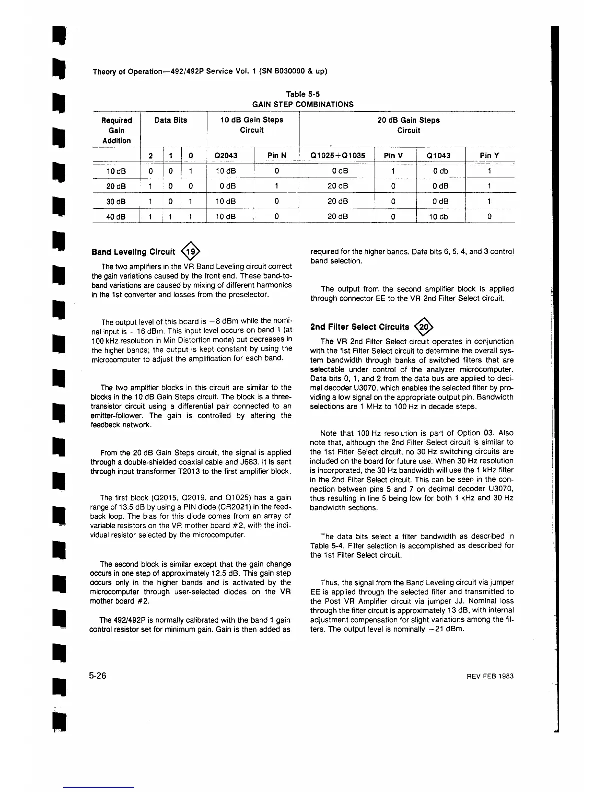
Table 5-5
GAIN STEP COMBINATIONS
Required
Gain
Addition
Data Bits
10 dB Gain Steps
Circuit
20 dB Gain Steps
Circuit
2
1 0 Q2043
Pin N
Q1025 + Q1035 Pin V
Q1043 Pin Y
10 dB 0
0
1 10 dB 0
OdB
1 0 db
1
20 dB
1
0
0
OdB
1
20 dB
0
OdB
1
30 dB
1
0
1 10 dB 0 20 dB
0
OdB 1
40 dB
1 1 1
10 dB 0 20 dB
0
10 db
0
l t <9>
Band Leveling Circuit
The two amplifiers in the VR Band Leveling circuit correct
the gain variations caused by the front end. These band-to-
band variations are caused by mixing of different harmonics
in the 1st converter and losses from the preselector.
required for the higher bands. Data bits 6, 5, 4, and 3 control
band selection.
The output from the second amplifier block is applied
through connector EE to the VR 2nd Filter Select circuit.
The output level of this board is - 8 dBm while the nomi
nal input is -1 6 dBm. This input level occurs on band 1 (at
100 kHz resolution in Min Distortion mode) but decreases in
the higher bands; the output is kept constant by using the
microcomputer to adjust the amplification for each band.
The two amplifier blocks in this circuit are similar to the
blocks in the 10 dB Gain Steps circuit. The block is a three-
transistor circuit using a differential pair connected to an
emitter-follower. The gain is controlled by altering the
feedback network.
From the 20 dB Gain Steps circuit, the signal is applied
through a double-shielded coaxial cable and J683. It is sent
through input transformer T2013 to the first amplifier block.
The first block (Q2015, Q2019, and Q1025) has a gain
range of 13.5 dB by using a PIN diode (CR2021) in the feed
back loop. The bias for this diode comes from an array of
variable resistors on the VR mother board #2, with the indi
vidual resistor selected by the microcomputer.
The second block is similar except that the gain change
occurs in one step of approximately 12.5 dB. This gain step
occurs only in the higher bands and is activated by the
microcomputer through user-selected diodes on the VR
mother board #2.
The 492/492P is normally calibrated with the band 1 gain
control resistor set for minimum gain. Gain is then added as
2nd Filter Select Circuits \20^
The VR 2nd Filter Select circuit operates in conjunction
with the 1 st Filter Select circuit to determine the overall sys
tem bandwidth through banks of switched filters that are
selectable under control of the analyzer microcomputer.
Data bits 0, 1, and 2 from the data bus are applied to deci
mal decoder U3070, which enables the selected filter by pro
viding a low signal on the appropriate output pin. Bandwidth
selections are 1 MHz to 100 Hz in decade steps.
Note that 100 Hz resolution is part of Option 03. Also
note that, although the 2nd Filter Select circuit is similar to
the 1st Filter Select circuit, no 30 Hz switching circuits are
included on the board for future use. When 30 Hz resolution
is incorporated, the 30 Hz bandwidth will use the 1 kHz filter
in the 2nd Filter Select circuit. This can be seen in the con
nection between pins 5 and 7 on decimal decoder U3070,
thus resulting in line 5 being low for both 1 kHz and 30 Hz
bandwidth sections.
The data bits select a filter bandwidth as described in
Table 5-4. Filter selection is accomplished as described for
the 1 st Filter Select circuit.
Thus, the signal from the Band Leveling circuit via jumper
EE is applied through the selected filter and transmitted to
the Post VR Amplifier circuit via jumper JJ. Nominal loss
through the filter circuit is approximately 13 dB, with internal
adjustment compensation for slight variations among the fil
ters. The output level is nominally —21 dBm.
5-26
REV FEB 1983
 Loading...