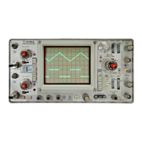
Theory of Operation—492/492P Service Vol. 1 (SN B030000 & up)
put of U4090D cause transistors Q6110, Q6090, and
Q6095 to conduct in sequence and add resistors R7096,
R7092, and R7093, respectively, in parallel to the feedback
path. The sequential adding of resistors into the feedback
path effectively reduces the gain of U4090D exponentially.
Although it may appear that such a system would result in
steps of gain resolution, the reaction characteristics of the
transistors smooth the transitions and result in a smooth
exponential gain curve.
Pulse Stretcher Circuit
The Pulse Stretch circuit, under control of the analyzer
microcomputer widens narrow peak signals to allow the
Digital Storage circuit time to acquire such signals. If this is
not done, the 9-microsecond digitizing rate of the Digital
Storage circuits is too short to acquire very narrow signals.
The circuits accomplish this function by stretching the fall
time of fast pulse signals. The circuit consists of FET switch
Q7110 and the associated components in the feedback path
of the output operational amplifier U4090C.
When pulse stretch mode is not selected (by data bit 7
from the analyzer data bus being a 0), FET switch Q7110 is
off. With Q7110 off, capacitor C7104 is not in the circuit and
the normal feedback path for U4090C and extra pulldown
current is provided through resistor R5108. This allows the
U4090C output to fall as fast as it rises.
When pulse stretch mode is selected (by data bit 7 being
a 1), FET switch Q7110 is turned on and capacitor C7104 is
inserted into the feedback circuit to slow the fall of the out
put. Also, the only pulldown current is through resistor
R5086. Diode CR7101 serves only to isolate the pulse
stretch circuit from the output circuit of the output amplifier.
Diode CR5101 turns on at low levels to prevent the amplifier
output from going too far negative and slowing the response
when the input changes. When the output of Q4100 swings
positive, the diode CR5101 disconnects. The primary ad
vantage of this circuit is that the operational amplifier re
moves offsets by controlling very closely the voltage at the
emitter of Q4100.
The Identify circuit permits the operator to check dis
played signals as true or spurious. This feature is imple
mented elsewhere in the analyzer, except for an offset that
is applied in the Video Amplifier. The test is accomplished by
changing the frequencies of the 1 st LO and the 2nd LO an
equal and opposite amount related to the harmonic number
used. If the signal is true, it will not move. As a check, the
display baseline of the signal that results from the frequency
is shifted about one division so the alternate display is right
below the other display.
Thus, if the display is two similar signals separated in
amplitude, the signal is true. This offset is inserted from the
analyzer data bus through latch U6050 and buffer U6060 to
the summing node of the output amplifier U4090C.
Digital Control Circuit
The Digital Control circuit provides the control signals for
selection of the various Video Amplifier functions and con
sists of address decoding, data latching, and buffering cir
cuits. From the analyzer data bus, address data and the
DATA VALID signal are applied to the address decoder
U6070 through edge connector pins 30, 26, 25, 27, 28, and
31. The decoder produces two enable signals that are ap
plied through inverter U5070 to gain latch U6040 and mode
latch U6050.
The Gain latch IC U6040, is an eight-bit latch that sup
plies command data to eight-bit digital-to-analog converter
U5041 to offset the Log Amplifier output signal. Mode latch
U6050 is an eight-bit latch that supplies command data
through buffer U6060 to select the resistors in the dB per
division switching circuit and to select identify, pulse stretch,
and log or linear mode.
VIDEO PROCESSOR
Refer to the block diagram adjacent to Diagram 23. The
Video Processor circuits perform band leveling, video filter
ing, and blanking. The circuits that perform these functions
are described in the following paragraphs.
Video Leveler Circuits
Video leveling compensates for those characteristics of
the analyzer front-end microwave circuits that cause unflat
response in band 4 (5.4 to 18 GHz). Since band 4 is a multi
plied band, any unflatness is accentuated. This leveling is
accomplished through a programmable perturbation of the
display baseline that is opposite in direction from the flat
ness error in the front-end circuits. As analyzer signal power
output decreases, the baseline rises an equal amount in
compensation; or, as power output increases, the baseline
falls an equal amount. The perturbation signal is actually
produced by a normalizer integrated circuit that produces 19
evenly spaced values of the input voltage, but with each
value corrected to compensate for unflatness.
The PRESELECTOR DRIVE signal from the 1st LO Driv
er circuits, is applied through edge connector pin 54 to an
input translation circuit that consists of two current drivers
(U3045A and half of Q3038, plus U3045B and the other half
of Q3038). Since the PRESELECTOR DRIVE signal is di
rectly related in amplitude to displayed analyzer frequency,
the nominal +10 V to — 10 V excursion voltage versus fre
quency curve in maximum span, relates to the full
bandwidth. This 20 volt maximum excursion is scaled to a
REV FEB 1983
5-35
 Loading...